L16 · Multiprocessors
Topic: multiprocessors · 75 pages
EECS 4340 Lecture 16 — Multiprocessors
Two Options to Make Computers Faster
Show slide text
If you want to make your computer faster, there are only two options:
Increase clock frequency- Execute two or more things in parallel
Instruction-Level Parallelism (ILP)- Programmer specified explicit parallelism
This slide frames the entire lecture. The crossed-out options — raising clock frequency and exploiting more instruction-level parallelism in a single core — are the two levers that have powered the prior lectures (pipelining, out-of-order, branch prediction, deep cache hierarchies). Both have hit physical and economic walls. Frequency scaling stalled around 2003–2005 because dynamic power P∝CV2f blew through reasonable thermal budgets, and lowering Vdd no longer worked because leakage grew exponentially as threshold voltages dropped. ILP, the topic of L05–L11, also saturates: real programs have limited dependence-free instruction windows, and dynamic scheduling structures like the reorder buffer and reservation stations scale super-linearly in area and power. The remaining option is explicit parallelism — multiple program counters running simultaneously on multiple cores. The rest of L16 explores how to expose, program, and keep coherent the resulting shared state.
Multiprocessors
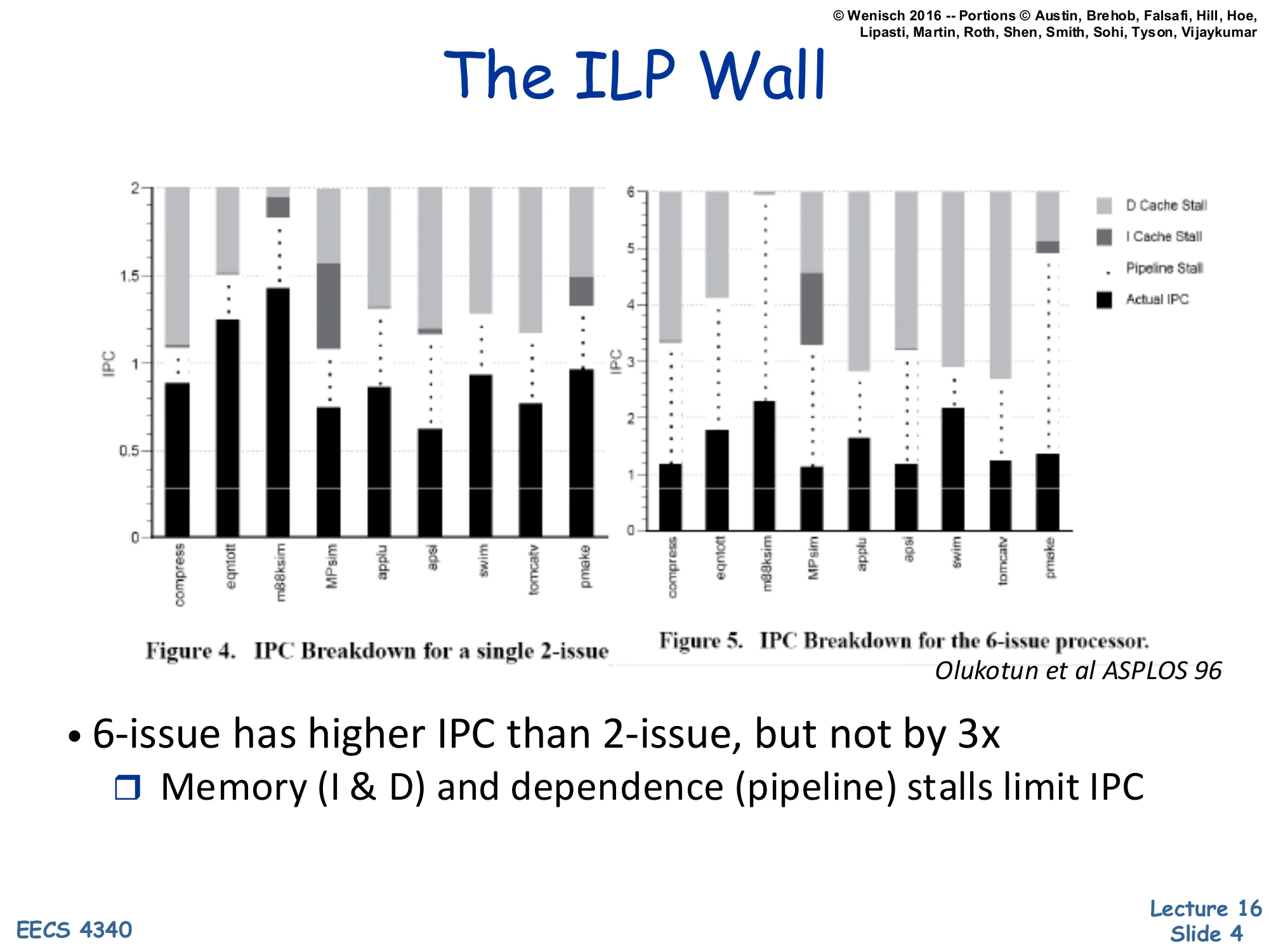
The ILP Wall
Show slide text
The ILP Wall
Figure 4. IPC Breakdown for a single 2-issue
Figure 5. IPC Breakdown for the 6-issue processor.
Olukotun et al ASPLOS 96
- 6-issue has higher IPC than 2-issue, but not by 3x
- Memory (I & D) and dependence (pipeline) stalls limit IPC
Olukotun’s 1996 ASPLOS paper measures actual IPC for a 2-issue and a 6-issue out-of-order processor across SPEC92-era benchmarks. Each stacked bar decomposes the cycle budget into actual retired instructions (black), pipeline-stall cycles, I-cache-miss stalls, and D-cache-miss stalls. Even tripling the issue width from 2 to 6 fails to triple sustained IPC: 2-issue averages around 0.8–1.0 IPC, while 6-issue only reaches roughly 1.2–2.3 IPC. The ceiling is set by cache misses — light-gray D-cache and dark-gray I-cache stall blocks dominate the unused issue slots — and by data-dependence chains that the reorder buffer cannot hide. This is the empirical core of the ILP wall: spending more transistors on a wider single-thread machine produces diminishing returns, because stalls (latency-bound, not parallelism-bound) become the bottleneck. The lesson motivates spending those transistors on additional cores instead of a wider single core.
Single-Thread Performance Trend
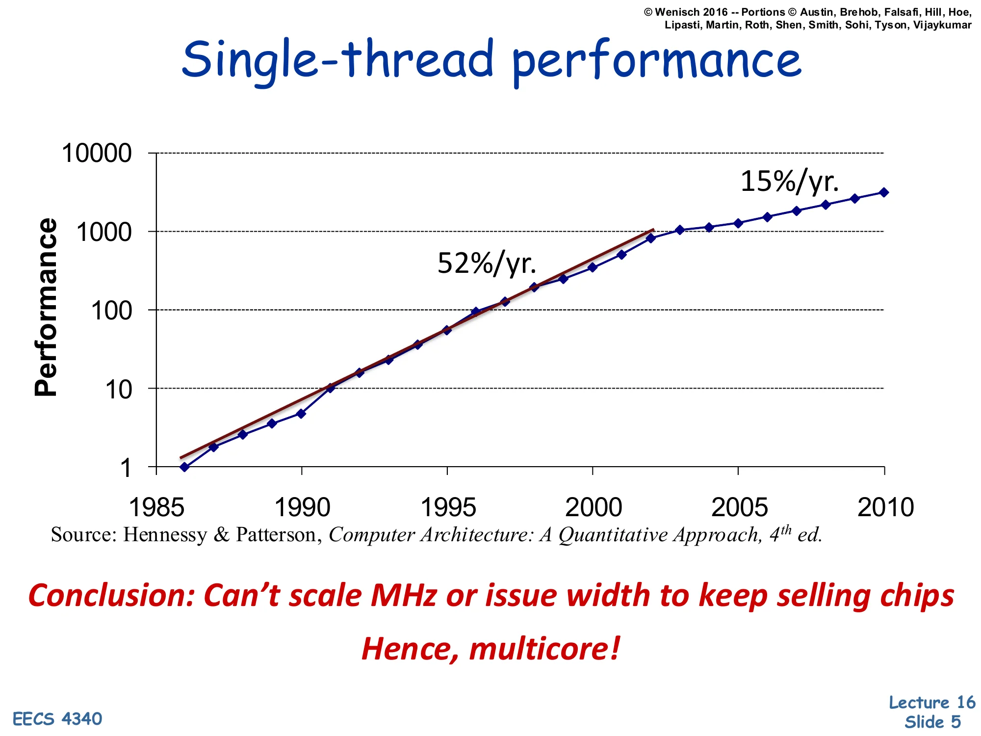
Show slide text
Single-thread performance
Performance vs. year (1985–2010, log scale).
- 52%/yr. growth from ~1986 to ~2003
- 15%/yr. growth from ~2003 onward
Source: Hennessy & Patterson, Computer Architecture: A Quantitative Approach, 4th ed.
Conclusion: Can’t scale MHz or issue width to keep selling chips
Hence, multicore!
This Hennessy & Patterson chart is the canonical ‘single-thread is dead’ graph. From 1986 through 2003, single-thread integer performance grew at a roughly 1.52n pace driven jointly by Dennard scaling (each CMOS generation gave more frequency at constant power density) and architectural ILP. After 2003, the slope flattens to about 15%/year because Dennard scaling broke: subthreshold leakage grew exponentially as Vt dropped, capping safe Vdd and therefore f, while ILP (last slide) saturated. The only way to keep applying Moore’s transistor budget productively is to spend it on replicated cores — more independent program counters per die. This pivot, around 2004–2006, is exactly when Intel and AMD shipped their first dual-core consumer chips. The course pivots here too: from squeezing one thread to coordinating many.
What Is a Parallel Computer?
Show slide text
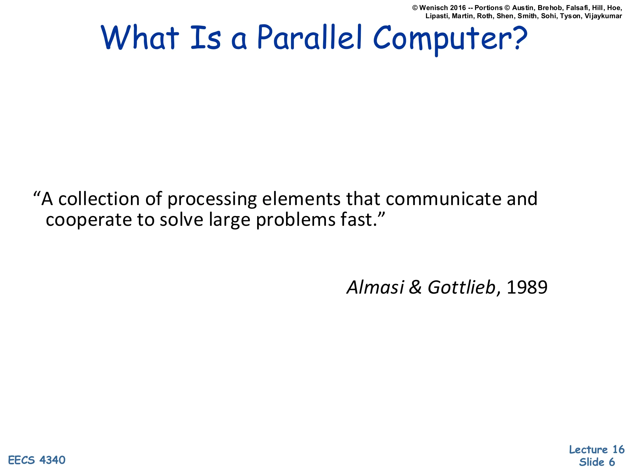
What Is a Parallel Computer?
“A collection of processing elements that communicate and cooperate to solve large problems fast.”
— Almasi & Gottlieb, 1989
The Almasi-Gottlieb definition is deliberately broad and useful. It pulls out three first-class concepts. First, processing elements — there are multiple of them, distinguishing parallel machines from any single-issue or single-superscalar processor. Second, communicate — the elements must exchange data, which immediately raises the question of shared memory vs. message passing (slides 13–17). Third, cooperate — they share a goal and therefore must synchronize, which raises locks, barriers, and coherence (slides 25–48). The qualifier ‘large problems fast’ reminds us that parallelism only helps when the problem has enough independent work to amortize communication and synchronization overhead — Amdahl’s law strikes again. This definition covers chip multiprocessors, server clusters, GPUs, and supercomputers under one umbrella, while excluding pipelined and superscalar processors that merely look parallel inside a single instruction stream.
Spectrum of Parallelism
Show slide text
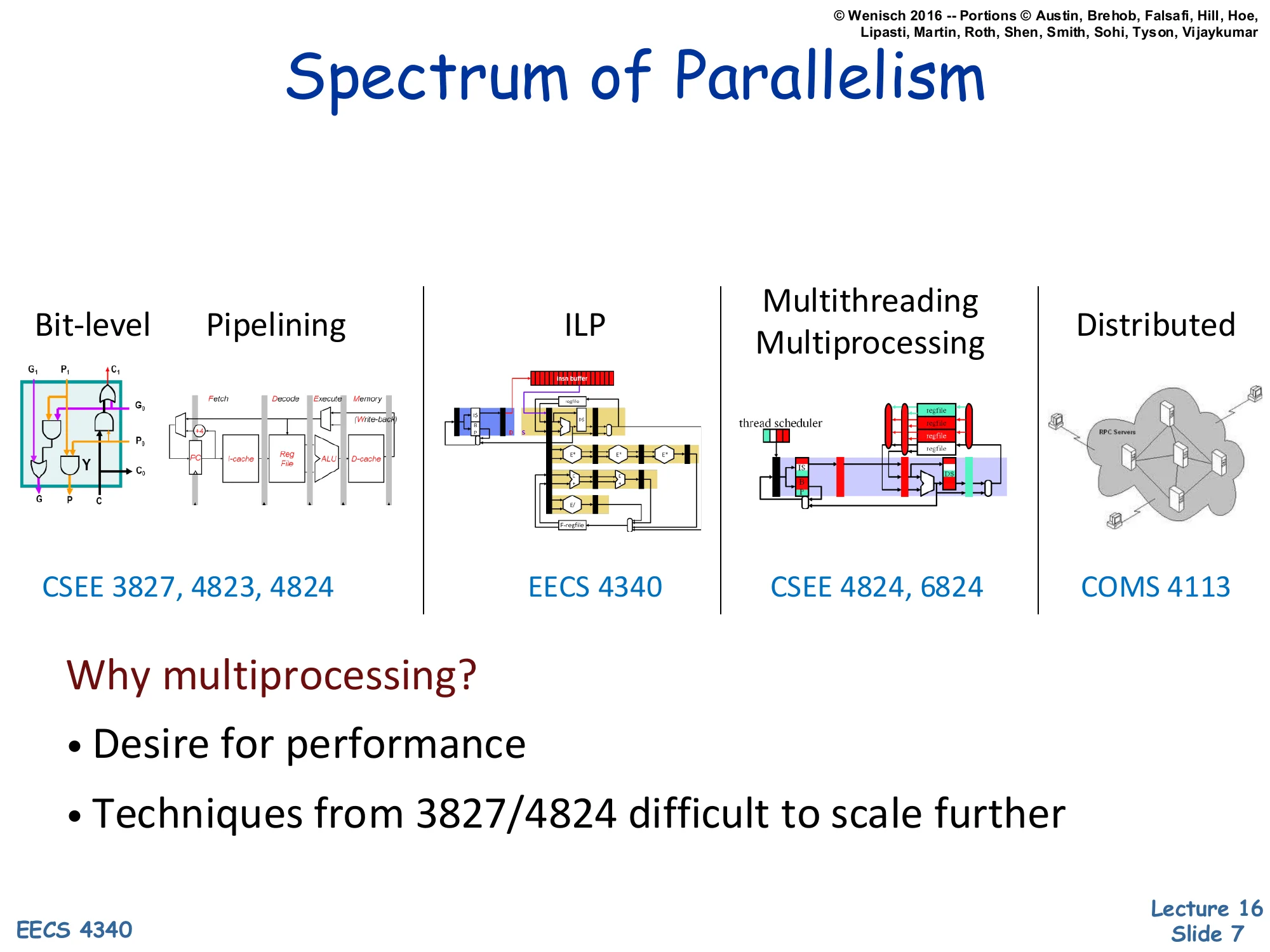
Spectrum of Parallelism
| Bit-level / Pipelining | ILP | Multithreading / Multiprocessing | Distributed |
|---|---|---|---|
| EECS 3827, 4823, 4340 | EECS 4340 | EECS 4340, 6824 | COMS 4113 |
Why multiprocessing?
- Desire for performance
- Techniques from 3827/4340 difficult to scale further
The slide places multiprocessing on a spectrum that ranges from finest-grain to coarsest-grain parallelism. Bit-level parallelism is what a 64-bit ALU does inside one cycle. Pipelining overlaps instructions in different stages. ILP (the heart of EECS 4340) issues multiple instructions per cycle from one stream via Tomasulo/ROB machinery. Multithreading and multiprocessing run multiple program counters within one chassis or chip. Distributed extends across machines coordinated by message passing. As you move right, the grain of parallelism gets coarser, the latency of communication grows, and the programmer has to take more explicit responsibility. The previous lectures in 4340 leaned heavily on the leftmost three; this lecture is the bridge from ILP to multiprocessing. The takeaway in red: ILP techniques scale poorly past 4–6 issue, so we step right on the spectrum.
Why Parallelism Now?
Show slide text
Why Parallelism Now?
- These arguments are no longer theoretical
- All major processor vendors are producing multicore chips
- Every machine will soon be a parallel machine
- All programmers will be parallel programmers???
- New software model
- Want a new feature? Hide the “cost” by speeding up the code first
- All programmers will be performance programmers???
- Some may eventually be hidden in libraries, compilers, and high level languages
- But a lot of work is needed to get there
- Big open questions:
- What will be the killer apps for multicore machines?
- How should the chips, languages, OS be designed to make it easier for us to develop parallel programs?
Wenisch is making the cultural argument that parallelism is no longer a niche concern for HPC researchers. Once vendors stop scaling per-thread performance, every shipped chip becomes a multicore — phones, laptops, servers — so every working programmer inherits the burden of either writing parallel code directly or trusting libraries, runtimes, and compilers to do it for them. The two open questions at the bottom are still genuinely open in 2026: ‘killer apps’ for parallelism turned out to be web servers, databases, ML training/inference, and graphics — not the desktop apps Wenisch’s slides anticipated — and language/OS support remains a moving target (CUDA, OpenMP, Rust async, etc.). For our purposes, the slide motivates the next blocks of the lecture: programming models (shared memory vs. message passing), synchronization, coherence, and consistency.
Multicore in Products
Show slide text
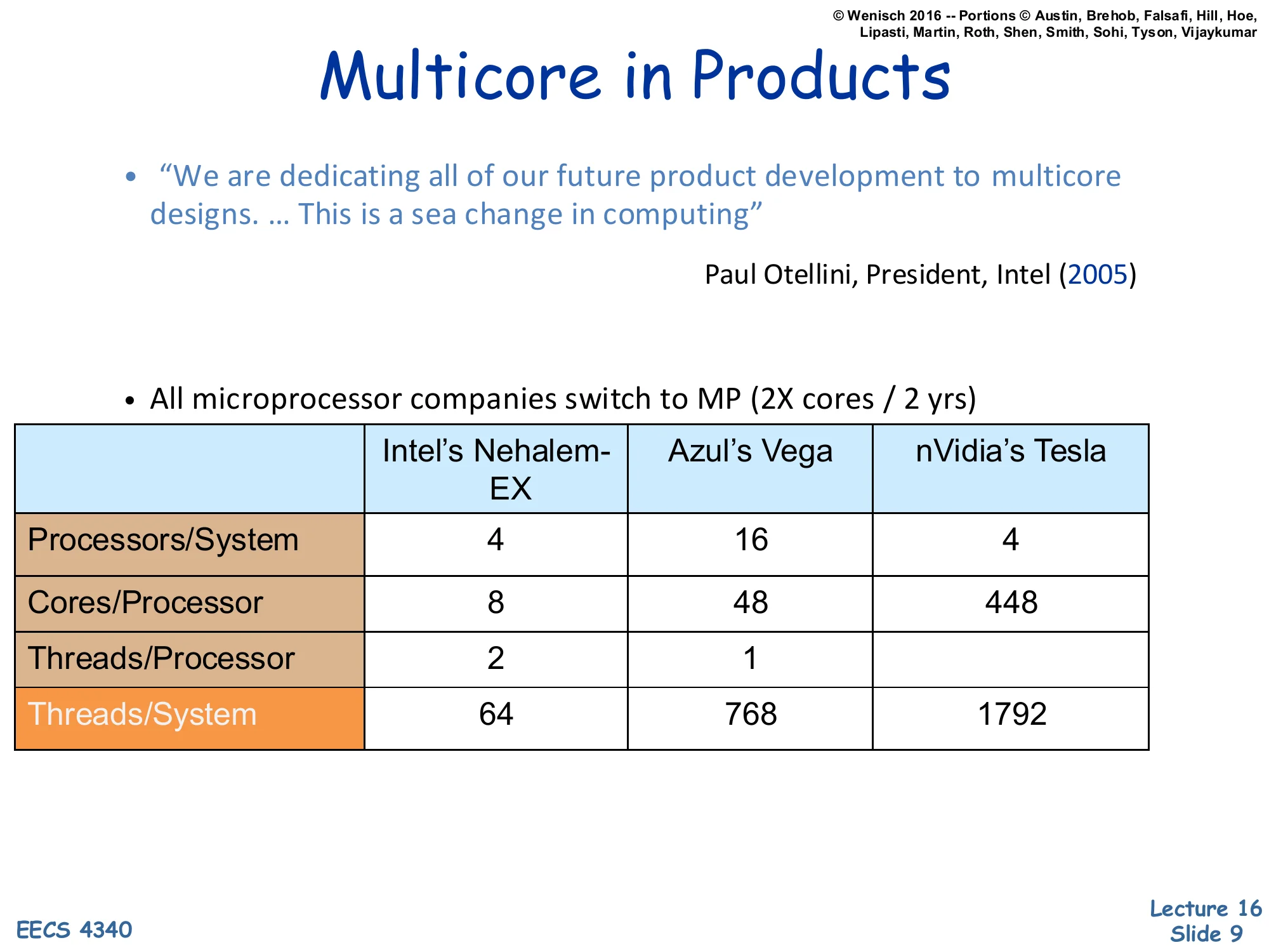
Multicore in Products
“We are dedicating all of our future product development to multicore designs. … This is a sea change in computing”
— Paul Otellini, President, Intel (2005)
- All microprocessor companies switch to MP (2X cores / 2 yrs)
| Intel’s Nehalem-EX | Azul’s Vega | nVidia’s Tesla | |
|---|---|---|---|
| Processors/System | 4 | 16 | 4 |
| Cores/Processor | 8 | 48 | 448 |
| Threads/Processor | 2 | 1 | |
| Threads/System | 64 | 768 | 1792 |
Otellini’s 2005 quote marks the official Intel pivot to multicore as a primary design axis. The table compares three contemporary points in the design space. Intel’s Nehalem-EX is a conventional server CPU with 8 cores and 2-way SMT per socket — modest core counts, beefy cores. Azul’s Vega is a Java-tuned server processor that trades single-thread performance for many simpler cores (48 per socket) to maximize aggregate throughput on garbage-collected workloads. nVidia’s Tesla is a GPU: 448 ‘cores’ per processor that are really SIMT lanes, ganged into warps. The columns are not directly comparable because ‘core’ means different things, but the right column shows the trend: aggregate hardware threads per system grew from tens to nearly 2000. The new axis of scaling is replication, not frequency or issue width — exactly the implication of the previous two slides.
Revolution Continues
Show slide text
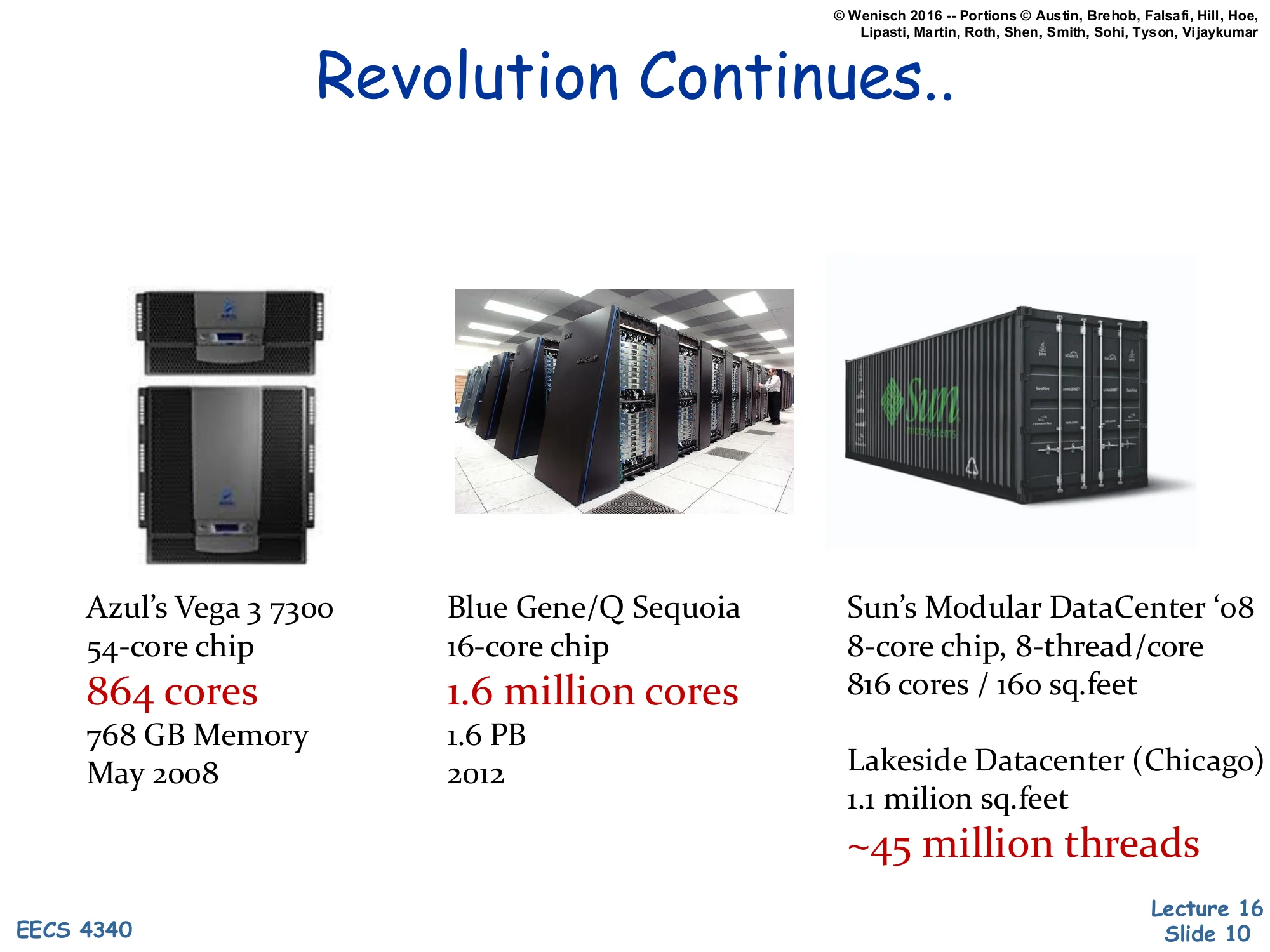
Revolution Continues..
- Azul’s Vega 3 7300 — 54-core chip, 864 cores, 768 GB Memory, May 2008
- Blue Gene/Q Sequoia — 16-core chip, 1.6 million cores, 1.6 PB, 2012
- Sun’s Modular DataCenter ‘08 — 8-core chip, 8-thread/core, 816 cores / 160 sq.feet
- Lakeside Datacenter (Chicago) — 1.1 million sq.feet, ~45 million threads
These four data points illustrate parallelism scaling at four very different granularities. Azul’s Vega 3 7300 packs 54 cores per chip with 16 chips per system for 864 cores — a single-rack appliance for managed-runtime workloads. Blue Gene/Q Sequoia, a 2012 LLNL supercomputer, reaches 1.6 million cores by replicating relatively simple PowerPC cores across hundreds of thousands of nodes connected by a 5-D torus network. Sun’s Modular DataCenter is a shipping container packed with servers — about 800 cores in 160 square feet of floor space — pioneering modular data-center design. Lakeside in Chicago, a 1.1 million-square-foot facility, packed into the tens-of-millions-of-threads regime by simply scaling the count of conventional servers. Together they show that multiprocessing is not just a chip-level phenomenon: the same coordination/coherence/consistency problems recur at every scale.
Multiprocessors Are Here To Stay
Show slide text
Multiprocessors Are Here To Stay
-
Moore’s law is making the multiprocessor a commodity part
- 1B transistors on a chip, what to do with all of them?
- Not enough ILP to justify a huge uniprocessor
- Really big caches? thit increases, diminishing %miss returns
-
Chip multiprocessors (CMPs)
- Every computing device (even your cell phone) is now a multiprocessor
The slide is the quantitative version of the earlier ‘why multicore’ argument. With ~1B transistors per chip in the late-2000s technology generation, designers face an allocation problem. They could build a huge uniprocessor with a wider issue, deeper ROB, and more aggressive speculation — but the IPC gains diminish (slide 4). They could pour the budget into really large caches — but as a cache grows, its hit time thit grows roughly as capacity, while miss-rate reductions get smaller per added MB. So neither lever scales linearly. The remaining productive use is to replicate cores. Chip multiprocessors (CMPs) — multiple complete cores integrated on one die — became the default architecture for everything from servers to smartphones. The cell-phone reference was prescient: by 2010, every mainstream phone shipped with a multicore SoC.
Concepts of Multiprocessors
Show slide text
Concepts of Multiprocessors
Parallel Programming Models
- Message passing, shared memory (pthreads and GPU)
Synchronization
- Locks, Lock-free structures, Transactional Memory
Coherency and Consistency
- Snooping and Directory-based Coherency
- Memory Consistency Models
Interconnection Networks
- On-chip and off-chip networks
Applications & Architectures
- Data center applications, MLPerf
Unconventional Parallel Architectures
- Dataflow architectures and systolic arrays
This is the lecture’s roadmap. Each bullet is a major topic the rest of the slides will cover in order. Parallel programming models cover how the programmer expresses parallelism — implicit shared loads/stores or explicit messages. Synchronization covers how parallel threads coordinate access to shared state — locks, barriers, flags, speculative transactional memory. Coherency keeps multiple cached copies of the same line consistent (snooping, directory protocols); consistency defines the ordering rules between accesses to different addresses. Interconnection networks are the physical substrate. Applications and architectures anchor the abstractions in real workloads. Unconventional architectures (dataflow, systolic) suggest that the von Neumann sequential model is not the only way to organize computation. The same outline reappears as the wrap-up slide 75.
Parallel Programming Models
Programming Model Elements
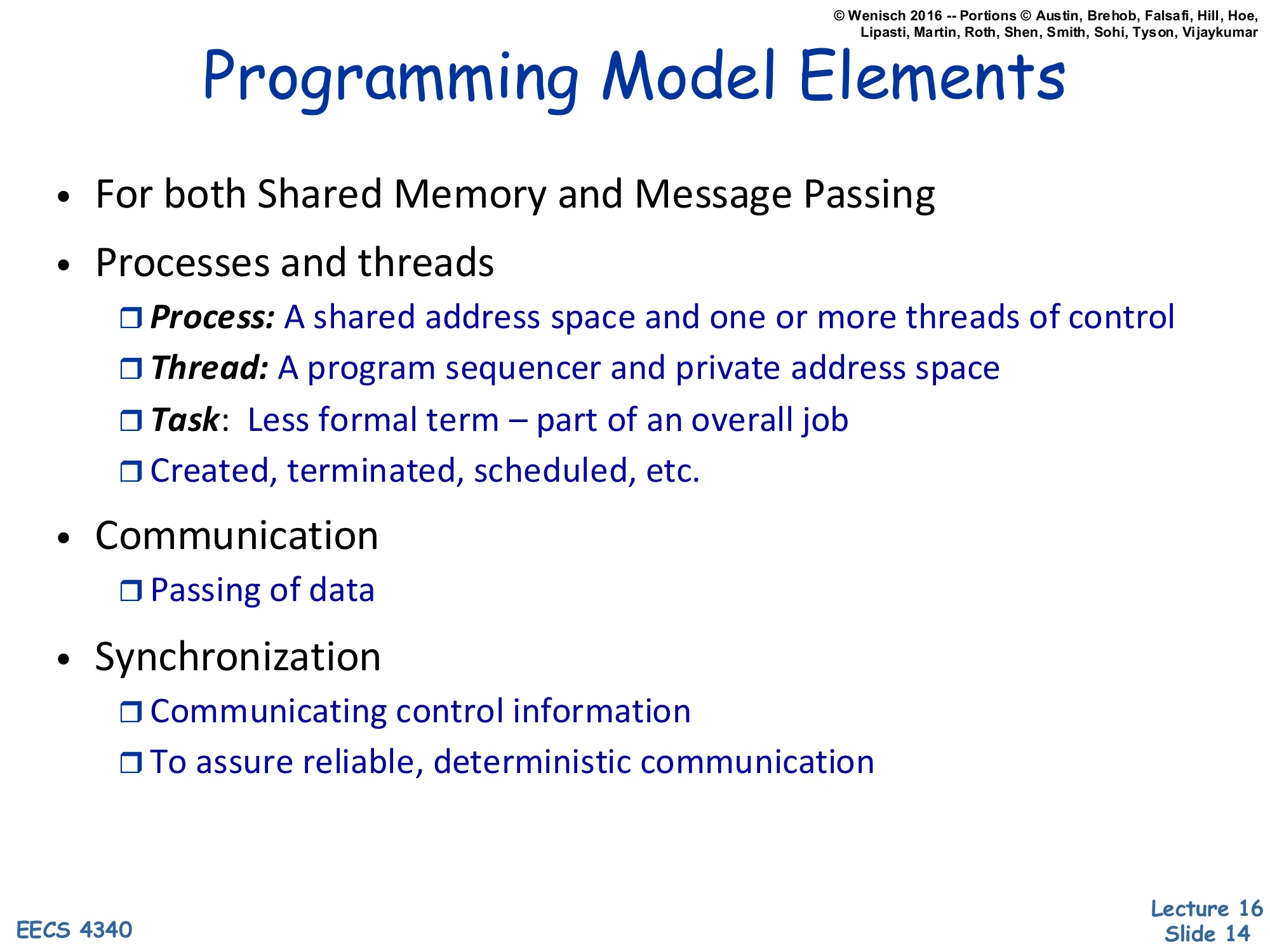
Show slide text
Programming Model Elements
- For both Shared Memory and Message Passing
- Processes and threads
- Process: A shared address space and one or more threads of control
- Thread: A program sequencer and private address space
- Task: Less formal term — part of an overall job
- Created, terminated, scheduled, etc.
- Communication
- Passing of data
- Synchronization
- Communicating control information
- To assure reliable, deterministic communication
This slide nails down vocabulary that the rest of the lecture takes for granted. A process is a heavy unit owning a shared address space (in Unix terms, the page tables, file descriptors, etc.) plus one or more threads. Each thread has its own program counter, register state, and stack — the ‘private address space’ phrasing here is slightly non-standard; what’s actually private is the stack and registers, while the heap and code are shared. Tasks are a deliberately informal term used in higher-level frameworks (OpenMP, Cilk, TBB) for chunks of work that can be scheduled. Two key activities crosscut both shared-memory and message-passing models: communication, which moves data between threads, and synchronization, which moves control information so that data movement is reliable and ordered. The next several slides unpack how shared memory makes communication implicit (loads/stores) and how message passing makes it explicit (send/recv).
Historical View — Three Architectures
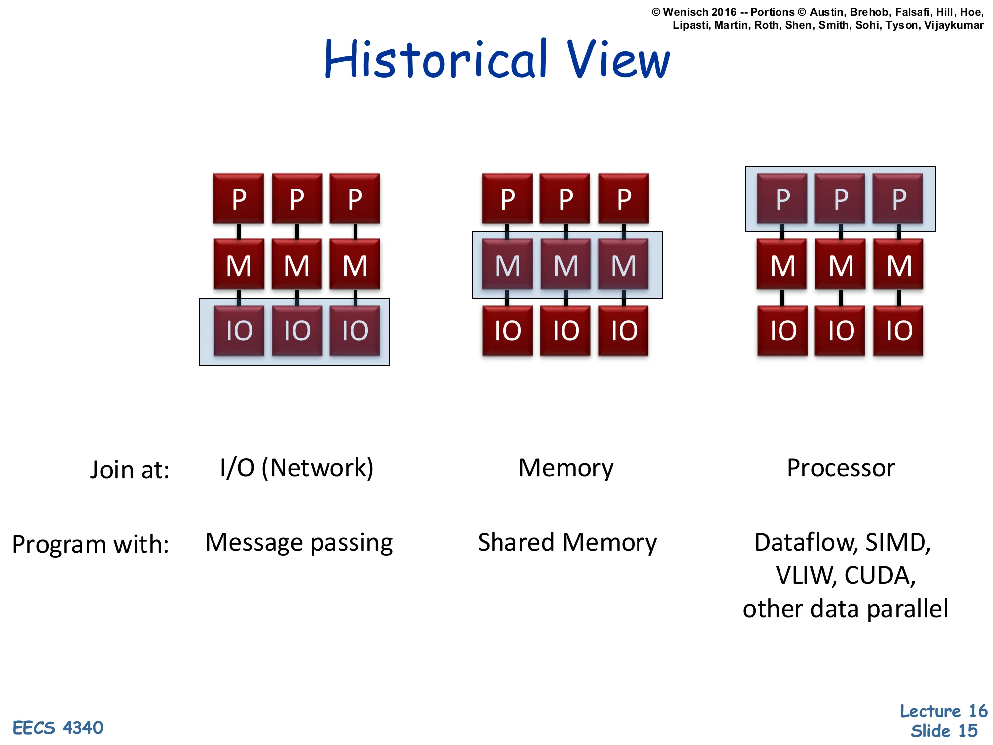
Show slide text
Historical View
Three configurations of P (processor), M (memory), IO blocks, distinguished by where the parallelism ‘joins’:
| Join at: | I/O (Network) | Memory | Processor |
|---|---|---|---|
| Program with: | Message passing | Shared Memory | Dataflow, SIMD, VLIW, CUDA, other data parallel |
The slide presents three textbook ‘machine archetypes’ classified by where the multiple processing elements share state. In the leftmost machine, each P has its own M and joins others only through I/O — this is a classical cluster or distributed system, programmed by message passing (MPI in HPC, RPC in distributed systems). In the middle machine, multiple Ps share a memory subsystem — the classical shared-memory multiprocessor, programmed with pthreads, OpenMP, or Java threads, and the focus of slides 16–48. On the right, multiple Ps share a single processing context (or share at the instruction-issue level) — this captures SIMD vector machines, VLIW, dataflow processors, and modern GPUs running CUDA. Notice that the classification axis is purely structural: where in the memory–compute hierarchy does sharing occur? That structural choice dictates the most natural programming model.
Shared-Memory Model
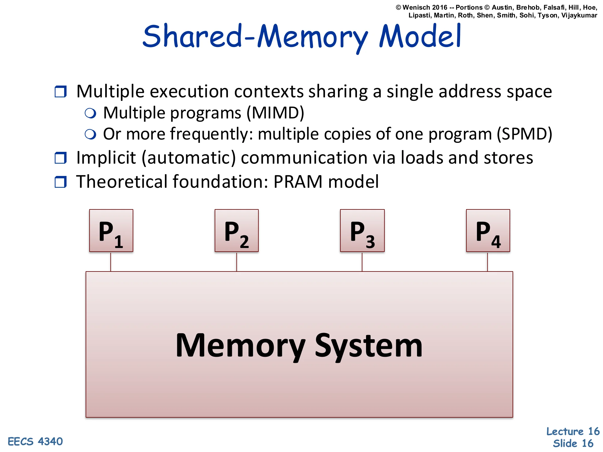
Show slide text
Shared-Memory Model
- Multiple execution contexts sharing a single address space
- Multiple programs (MIMD)
- Or more frequently: multiple copies of one program (SPMD)
- Implicit (automatic) communication via loads and stores
- Theoretical foundation: PRAM model
Diagram: P₁, P₂, P₃, P₄ all connected to a single Memory System.
Shared memory is the dominant model for chip multiprocessors and SMPs. All processors see one global address space; they communicate by writing to and reading from agreed-upon addresses. Two execution-style flavors are noted: MIMD (Multiple Instruction streams, Multiple Data) means each processor runs an arbitrary program, while SPMD (Single Program, Multiple Data) means all processors run the same binary but branch on a thread ID — this is the common case in scientific computing and OpenMP. Communication is implicit — there is no explicit send instruction; a store on one core eventually becomes visible to a load on another core, mediated by cache coherence and the memory consistency model. The PRAM (Parallel Random Access Machine) is the theoretical idealization where every processor reads or writes any global memory location in unit time — a useful abstraction for algorithm analysis but not achievable in real hardware.
Global Shared Physical Address Space
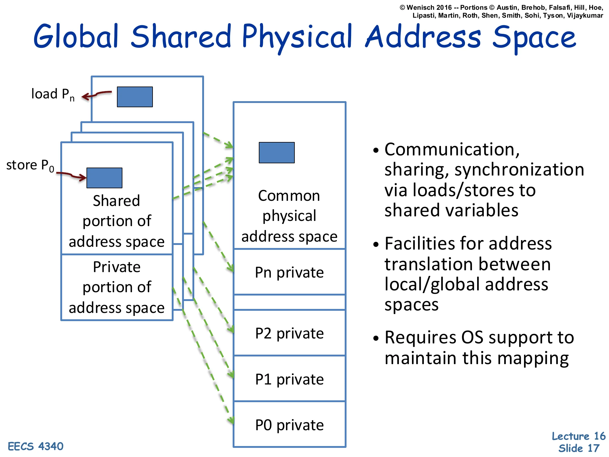
Show slide text
Global Shared Physical Address Space
Each process has a Shared portion of address space and a Private portion of address space. Loads from Pn and stores from P0 map (via dashed arrows) into a Common physical address space, which contains a shared region plus per-process private regions (P0 private … Pn private).
- Communication, sharing, synchronization via loads/stores to shared variables
- Facilities for address translation between local/global address spaces
- Requires OS support to maintain this mapping
This slide shows how shared memory is implemented on top of conventional virtual memory. Each process retains a private virtual address space, but a designated shared portion of each process’s VA range is mapped — by the OS, via the page tables — to the same physical frames. The dashed green arrows in the figure show that a store from P0‘s shared region and a load from Pn‘s shared region resolve to the same physical address, providing a communication channel. The OS plays three roles: it allocates the shared physical region (e.g., shmget/mmap), it sets up the per-process VA-to-PA mappings, and it maintains protection so private regions stay private. From the programmer’s perspective, all the address-translation gymnastics are invisible: a pointer is a pointer, and *p = 5 in one thread eventually becomes visible to another thread that reads *p. Coherence (slides 31–48) ensures the timing and value semantics are correct.
Why Shared Memory?
Show slide text
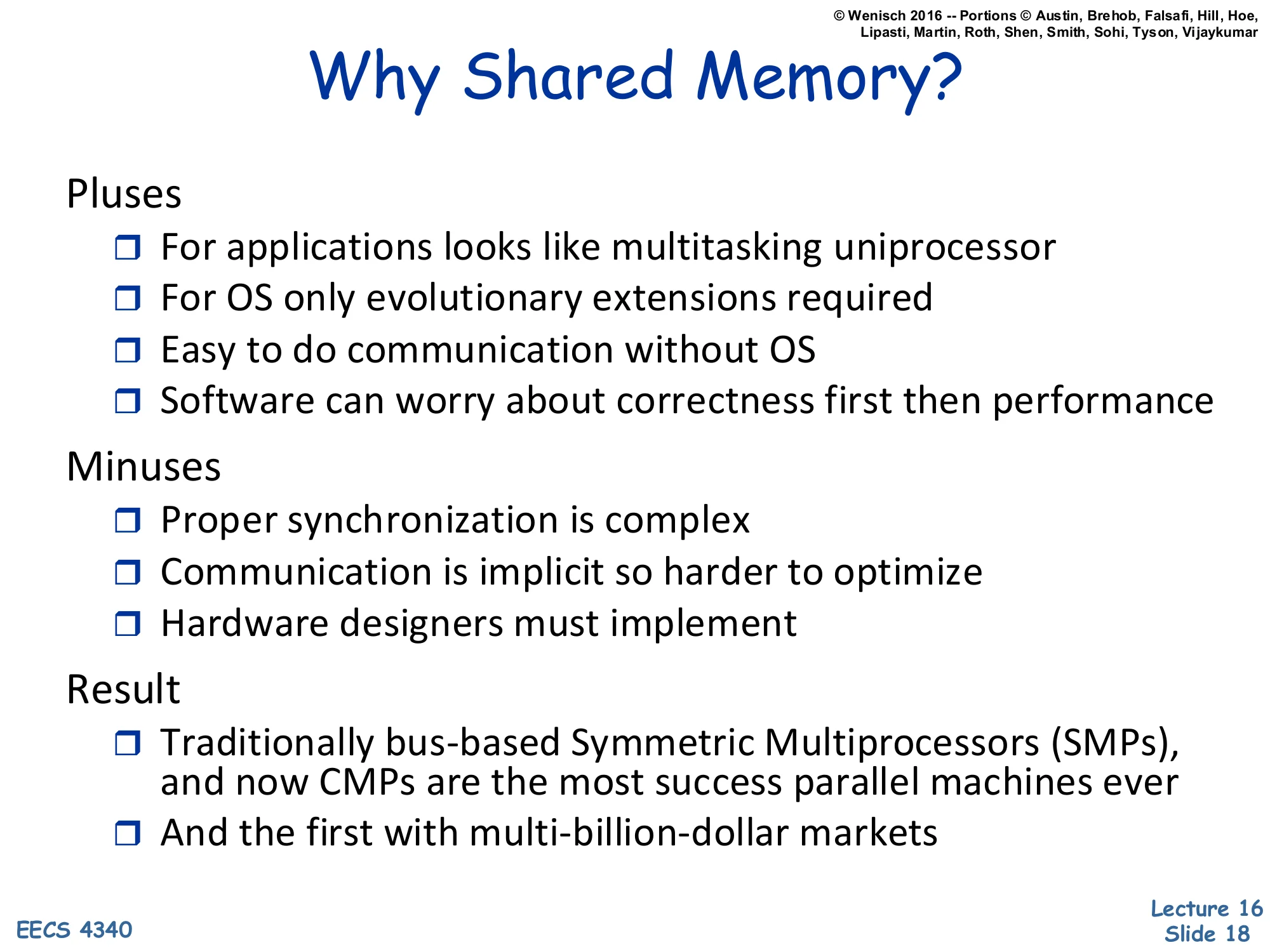
Why Shared Memory?
Pluses
- For applications looks like multitasking uniprocessor
- For OS only evolutionary extensions required
- Easy to do communication without OS
- Software can worry about correctness first then performance
Minuses
- Proper synchronization is complex
- Communication is implicit so harder to optimize
- Hardware designers must implement
Result
- Traditionally bus-based Symmetric Multiprocessors (SMPs), and now CMPs are the most success parallel machines ever
- And the first with multi-billion-dollar markets
Shared memory dominates because it minimizes programmer pain at the cost of hardware pain. The pluses say: applications and OS only need evolutionary changes (Unix processes already share kernel data structures; just add threads), there’s no kernel-mediated send/recv on the fast path, and a programmer can write a sequential algorithm and parallelize incrementally. The minuses are real: synchronization correctness (race conditions, deadlocks, ABA bugs) is famously hard; implicit communication makes performance pathologies like false sharing invisible to the programmer; and the hardware has to enforce coherence across many cores. The historical result: bus-based SMPs (Sun Enterprise, Sequent) ruled the 1990s server market; CMPs (every Intel/AMD/Arm multicore since ~2005) inherit and extend the model. Message passing exists (MPI, distributed systems) but never dominated commodity computing because the productivity case for shared memory is overwhelming.
Graphics Processing Units (GPU)
Show slide text
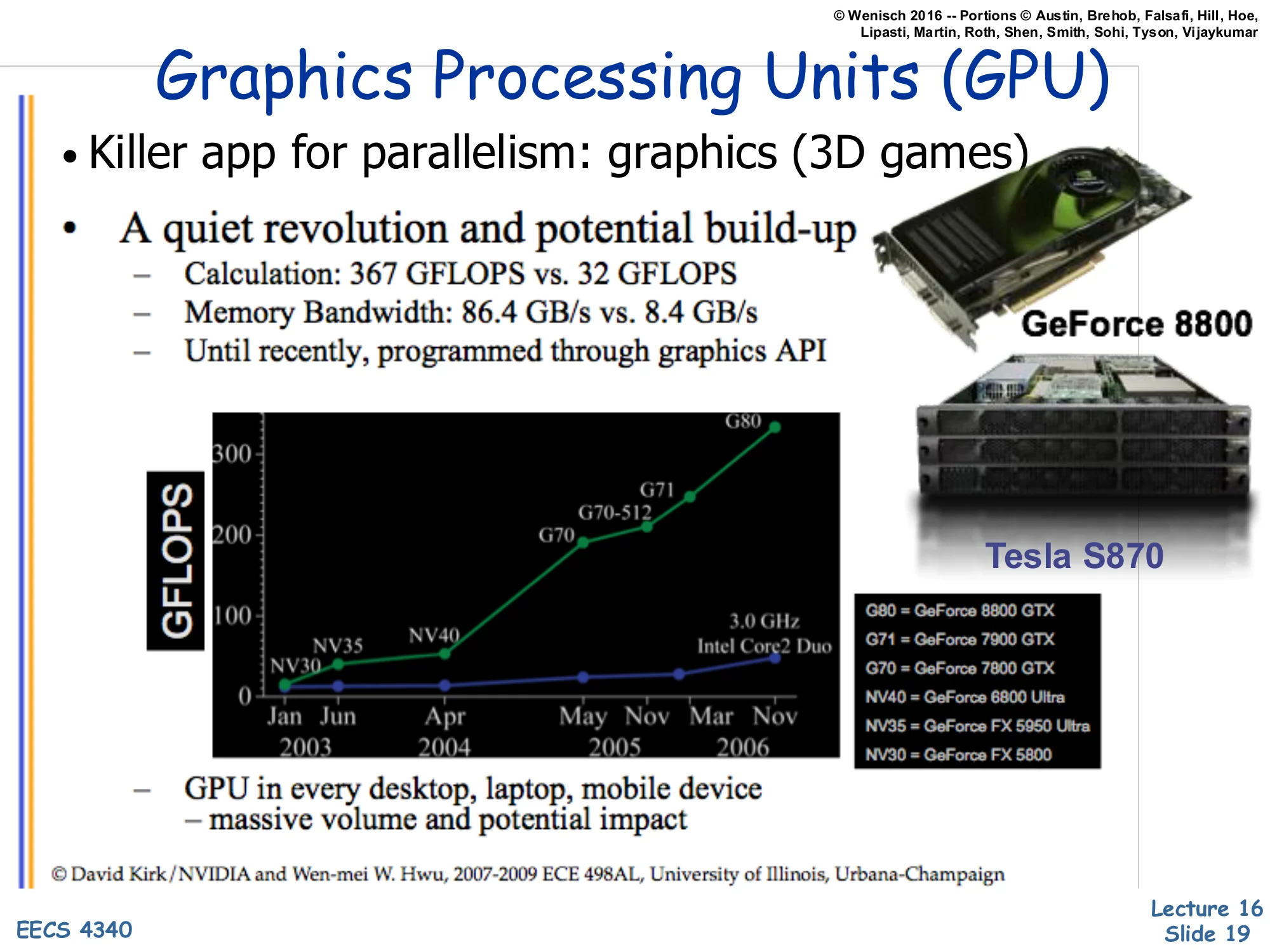
Graphics Processing Units (GPU)
- Killer app for parallelism: graphics (3D games)
- A quiet revolution and potential build-up
- Calculation: 367 GFLOPS vs. 32 GFLOPS
- Memory Bandwidth: 86.4 GB/s vs. 8.4 GB/s
- Until recently, programmed through graphics API
GFLOPS chart: NV30, NV35, NV40, G70, G70-512, G80 (NVIDIA) compared to 3.0 GHz Intel Core2 Duo, Jun 2003 – Nov 2006. Pictured: GeForce 8800, Tesla S870.
- GPU in every desktop, laptop, mobile device — massive volume and potential impact
© David Kirk/NVIDIA and Wen-mei W. Hwu, 2007–2009 ECE 498AL, University of Illinois, Urbana-Champaign
GPUs entered the parallel-computing conversation through the back door. Their original purpose — rasterizing 3D graphics for games — happens to be embarrassingly parallel: shading a million pixels per frame is a million independent computations on different data. The slide quotes G80-class numbers: 367 GFLOPS sustained, 86.4 GB/s memory bandwidth — roughly 11× and 10× a contemporary high-end Intel CPU. GPUs achieved this by spending almost all of their transistor budget on ALUs and very little on caches, branch predictors, or out-of-order machinery (next slide makes this concrete). For most of the 2000s, programmers had to express their computation as graphics shaders to use a GPU — awkward but possible (the ‘GPGPU’ era). The volume argument is economic: GPUs ship in every consumer device, so per-unit cost amortizes R&D, and that volume drove the GPU into HPC, ML, and finally into general-purpose compute via CUDA/OpenCL.
What is Behind such an Evolution?
Show slide text
What is Behind such an Evolution?
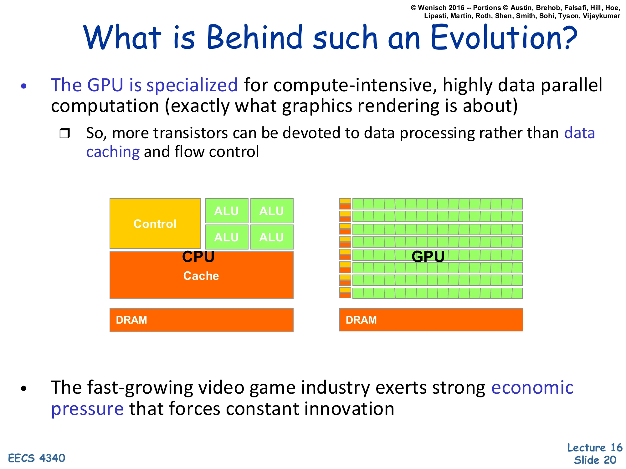
- The GPU is specialized for compute-intensive, highly data parallel computation (exactly what graphics rendering is about)
- So, more transistors can be devoted to data processing rather than data caching and flow control
Diagram: CPU has a small number of large ALUs, a Control block, a big Cache, and DRAM. GPU has many small ALUs in a grid, very small control/cache slivers, and DRAM.
- The fast-growing video game industry exerts strong economic pressure that forces constant innovation
The CPU vs. GPU floor-plan cartoon makes the architectural philosophy concrete. A CPU spends a large fraction of die area on control (front-end, decode, reorder buffer, scheduler) and cache (multilevel hierarchy with hardware-managed coherence) so that a single thread runs as fast as possible despite irregular memory and branches. A GPU inverts the priorities: minimal cache, minimal control logic, but rows and rows of ALUs. The bet is that the workload — pixel shading, then later linear algebra and convolutions — has so much data parallelism that latencies can be hidden by thread-level oversubscription rather than by a sophisticated branch predictor or caches. The economic engine is the gaming industry: the multi-billion-dollar consumer market funds rapid iteration, which is why GPU peak FLOPS outpaced CPU FLOPS by an order of magnitude. This same architectural philosophy now powers ML accelerators.
GPUs and SIMD/Vector Data Parallelism
Show slide text
GPUs and SIMD/Vector Data Parallelism
- Graphics processing units (GPUs)
- How do they have such high peak FLOPS?
- Exploit massive data parallelism
- “SIMT” execution model
- Single instruction multiple threads
- Similar to both “vectors” and “SIMD”
- A key difference: better support for conditional control flow
- Program it with CUDA or OpenCL
- Extensions to C
- Perform a “shader task” (a snippet of scalar computation) over many elements
- Internally, GPU uses scatter/gather and vector mask operations
The GPU’s execution model — SIMT, Single Instruction Multiple Threads — is similar enough to SIMD and vector processing that the differences matter. A vector machine fetches one instruction and applies it to all lanes of a vector register. A SIMD machine does the same in a wider word. SIMT also runs one instruction across many lanes (a ‘warp’ on NVIDIA hardware, typically 32 lanes), but the programmer writes scalar code per thread, and the hardware groups threads into warps automatically. The crucial advantage is conditional control flow: when threads in a warp diverge on a branch, the hardware uses predication (a vector mask) to disable lanes that took the other path, then re-enables them when the paths reconverge. CUDA and OpenCL expose this as a C-like language where each kernel is the per-thread scalar program, and the runtime distributes thousands of threads across the GPU’s compute units.
Context: History of Programming GPUs
Show slide text
Context: History of Programming GPUs
- “GPGPU”
- Originally could only perform “shader” computations on images
- So, programmers started using this framework for computation
- Puzzle to work around the limitations, unlock the raw potential
- As GPU designers notice this trend…
- Hardware provided more “hooks” for computation
- Provided some limited software tools
- GPU designs are now fully embracing compute
- More programmability features to each generation
- Industrial-strength tools, documentation, tutorials, etc.
- Can be used for in-game physics, etc.
- A major initiative to push GPUs beyond graphics (HPC)
GPGPU — General-Purpose computing on GPUs — describes the period (~2002–2007) when researchers smuggled scientific computations into pixel shaders, encoding matrices as textures and running fragment programs to do the math. The contortion was real but the speedups were already 10× over CPUs for embarrassingly parallel workloads, and that was enough to attract NVIDIA’s attention. NVIDIA responded with first the G80 architecture (2006) and CUDA (2007), then progressively more general programmability — atomic operations, shared scratchpad memory, double precision, unified address spaces — until by the time CUDA 6 (2014) GPUs were essentially a coprocessor accessible from C/C++ with all the affordances expected. Today the trend has continued into purpose-built ML accelerators (TPUs, NVIDIA Hopper/Blackwell tensor cores) where matrix multiplication is the first-class primitive.
History of GPU Architectures
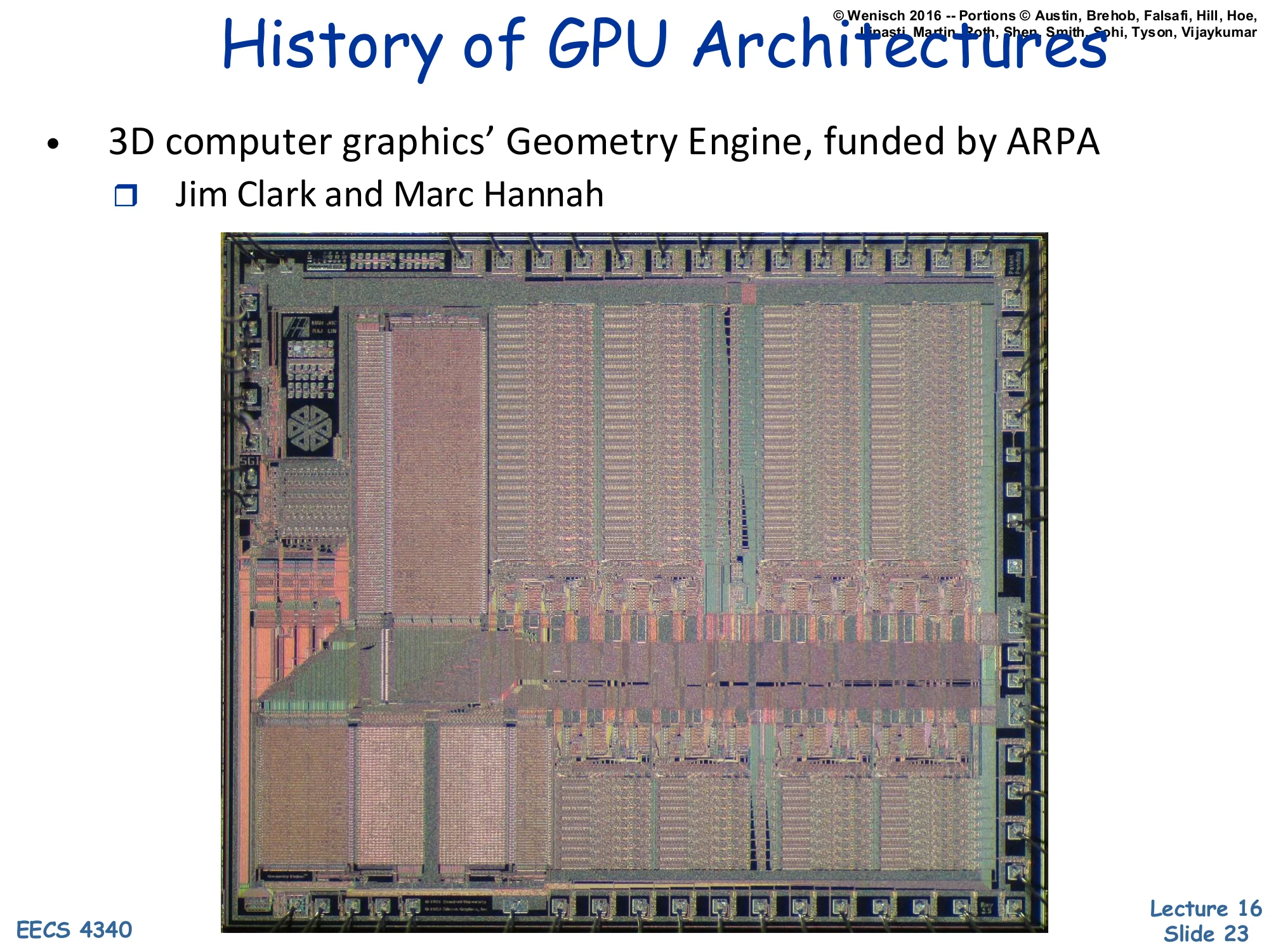
Show slide text
History of GPU Architectures
- 3D computer graphics’ Geometry Engine, funded by ARPA
- Jim Clark and Marc Hannah
Image: a die photo of an early Geometry Engine chip.
The Geometry Engine, designed by Jim Clark and Marc Hannah at Stanford in the early 1980s with ARPA funding, is the architectural ancestor of today’s GPUs. It was a custom VLSI chip that performed the matrix-multiply pipeline used to transform 3D vertices into 2D screen coordinates: model-to-world, world-to-camera, perspective projection, viewport mapping. By offloading these floating-point matrix operations from the CPU, the Geometry Engine made interactive 3D graphics feasible on workstations. Clark went on to found Silicon Graphics (SGI) on the back of this work, and SGI’s IRIS and Onyx workstations dominated 3D graphics through the 1990s. The lineage from Geometry Engine to modern NVIDIA GPUs is direct: a fixed-function 3D pipeline gradually became programmable (vertex shaders → fragment shaders → unified shaders → CUDA cores).
GPU Architectures — NVIDIA G80
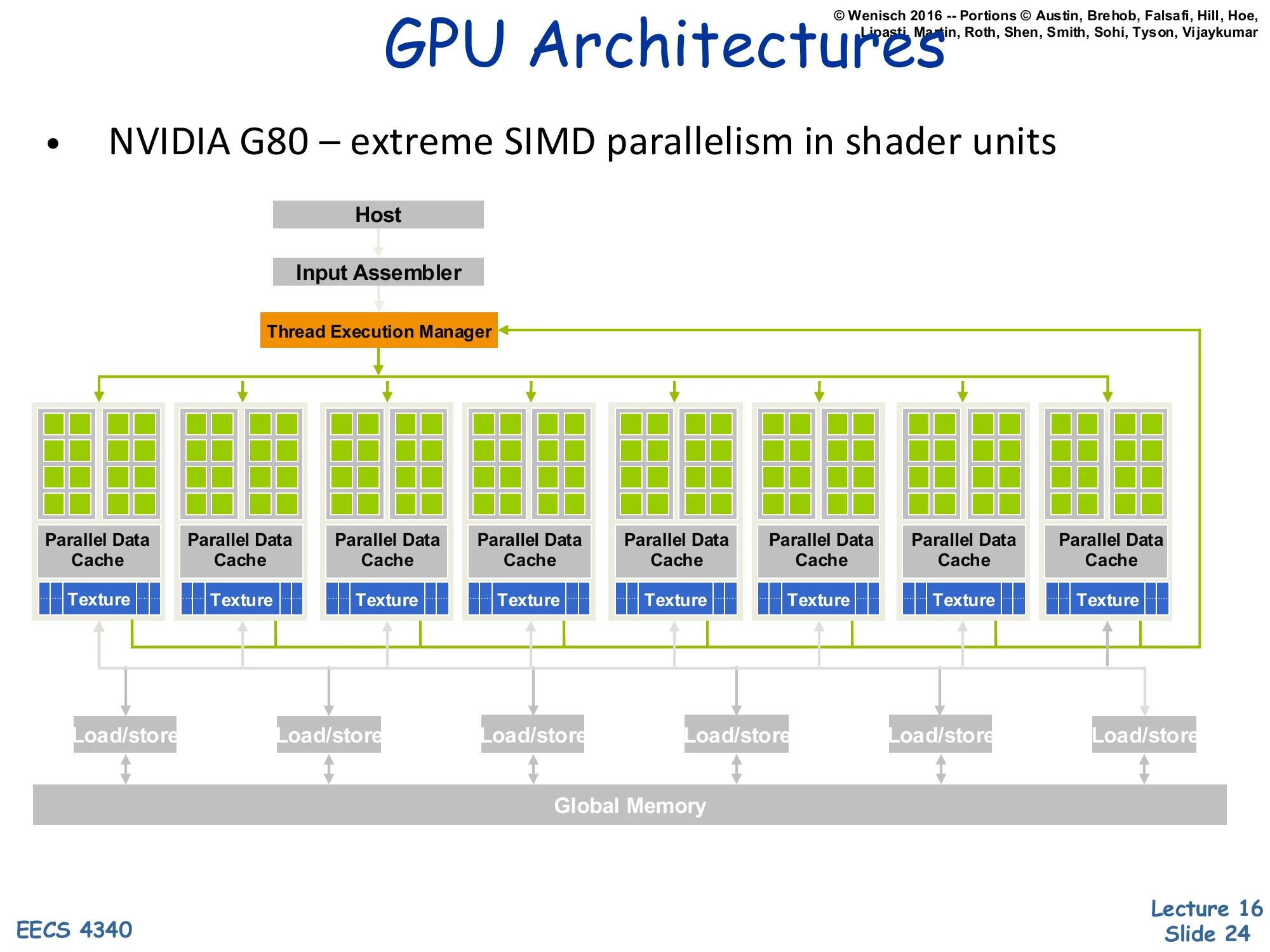
Show slide text
GPU Architectures
- NVIDIA G80 — extreme SIMD parallelism in shader units
Block diagram: Host → Input Assembler → Thread Execution Manager. Eight Parallel Data Cache + Texture units arranged in a row, each containing many shader cores. Each unit’s Load/store ports connect down to shared Global Memory.
The G80 (GeForce 8800, 2006) is the first NVIDIA architecture exposed to general-purpose computing through CUDA. The block diagram shows the structural ideas that survive in modern GPUs: a host interface that accepts work from the CPU, an input assembler that builds primitives, and a thread execution manager (warp scheduler) that dispatches groups of threads to compute units. Each compute unit (the green-block columns) bundles many simple ALU cores, a parallel data cache (the precursor of CUDA’s shared memory / today’s L1 plus shared scratchpad), and a texture unit (read-only filtering cache). All units share a global memory through load/store ports — this global memory is high-bandwidth GDDR/HBM, accessed at hundreds of GB/s. The architecture is essentially a many-core SIMT machine where the on-chip network ties together many simple cores, much closer to a distributed-memory many-core than to a classical SMP.
Synchronization
Synchronization Objectives
Show slide text
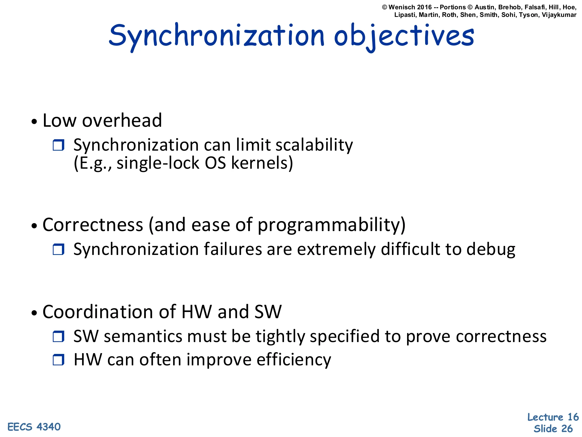
Synchronization objectives
- Low overhead
- Synchronization can limit scalability (E.g., single-lock OS kernels)
- Correctness (and ease of programmability)
- Synchronization failures are extremely difficult to debug
- Coordination of HW and SW
- SW semantics must be tightly specified to prove correctness
- HW can often improve efficiency
Synchronization is the discipline of getting threads to agree on order without sequentializing the whole machine. The first objective, low overhead, is the classic scaling concern: a single big kernel lock (BKL) on early-2000s Linux limited multicore scalability for years before fine-grained locking and read-copy-update were introduced. The second objective, correctness, is sobering — concurrency bugs are timing-dependent, often invisible until production load, and disproportionately responsible for the most expensive incidents in shipping software. The third objective demands tight HW/SW coordination: the language’s memory model (C11 atomics, Java JMM) and the hardware’s memory consistency model must match, or programmers can’t reason about whether their lock-free code works. Hardware can accelerate some primitives (e.g., load-linked/store-conditional, hardware transactional memory) but the contract must be precise.
Synchronization Forms
Show slide text
Synchronization Forms
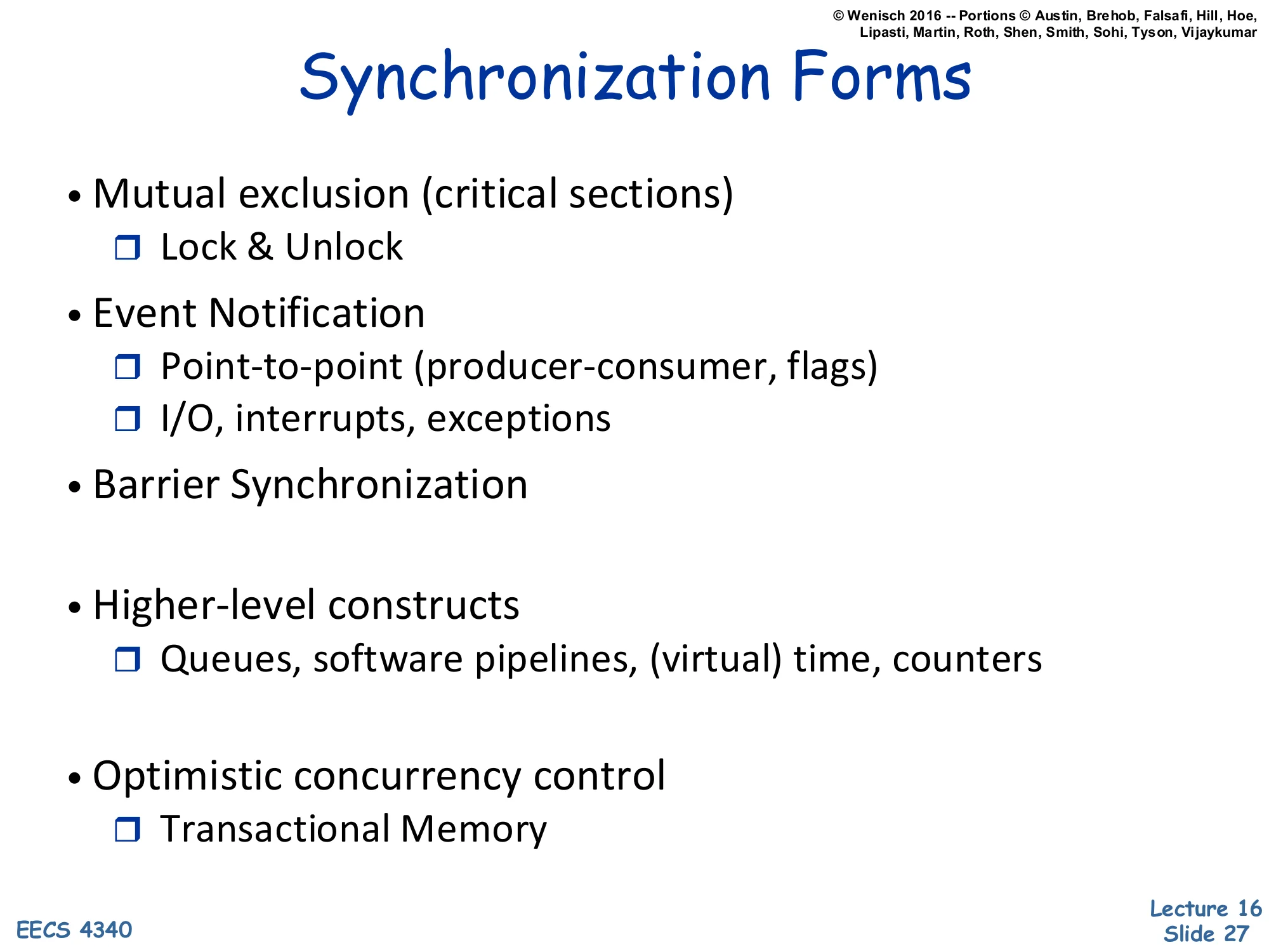
- Mutual exclusion (critical sections)
- Lock & Unlock
- Event Notification
- Point-to-point (producer-consumer, flags)
- I/O, interrupts, exceptions
- Barrier Synchronization
- Higher-level constructs
- Queues, software pipelines, (virtual) time, counters
- Optimistic concurrency control
- Transactional Memory
The synchronization forms tile the design space. Mutual exclusion uses a lock to serialize access to a critical section — only one thread inside at a time. Event notification is one-directional: a producer signals that work is ready, a consumer waits and proceeds. Barrier synchronization requires all participating threads to reach the barrier before any may proceed — used in bulk-synchronous parallel algorithms (BSP, MapReduce). Higher-level constructs layer on top: lock-free queues, software pipelines, virtual-time clocks for distributed systems. Optimistic concurrency control via transactional memory speculates that critical sections will not conflict and rolls back when they do — exposing more parallelism when contention is rare. The right primitive depends on the access pattern: locks excel for low-contention mutual exclusion, barriers for phase synchronization, and transactional memory for short, mostly-disjoint critical sections.
Anatomy of a Synchronization Op
Show slide text
Anatomy of a Synchronization Op
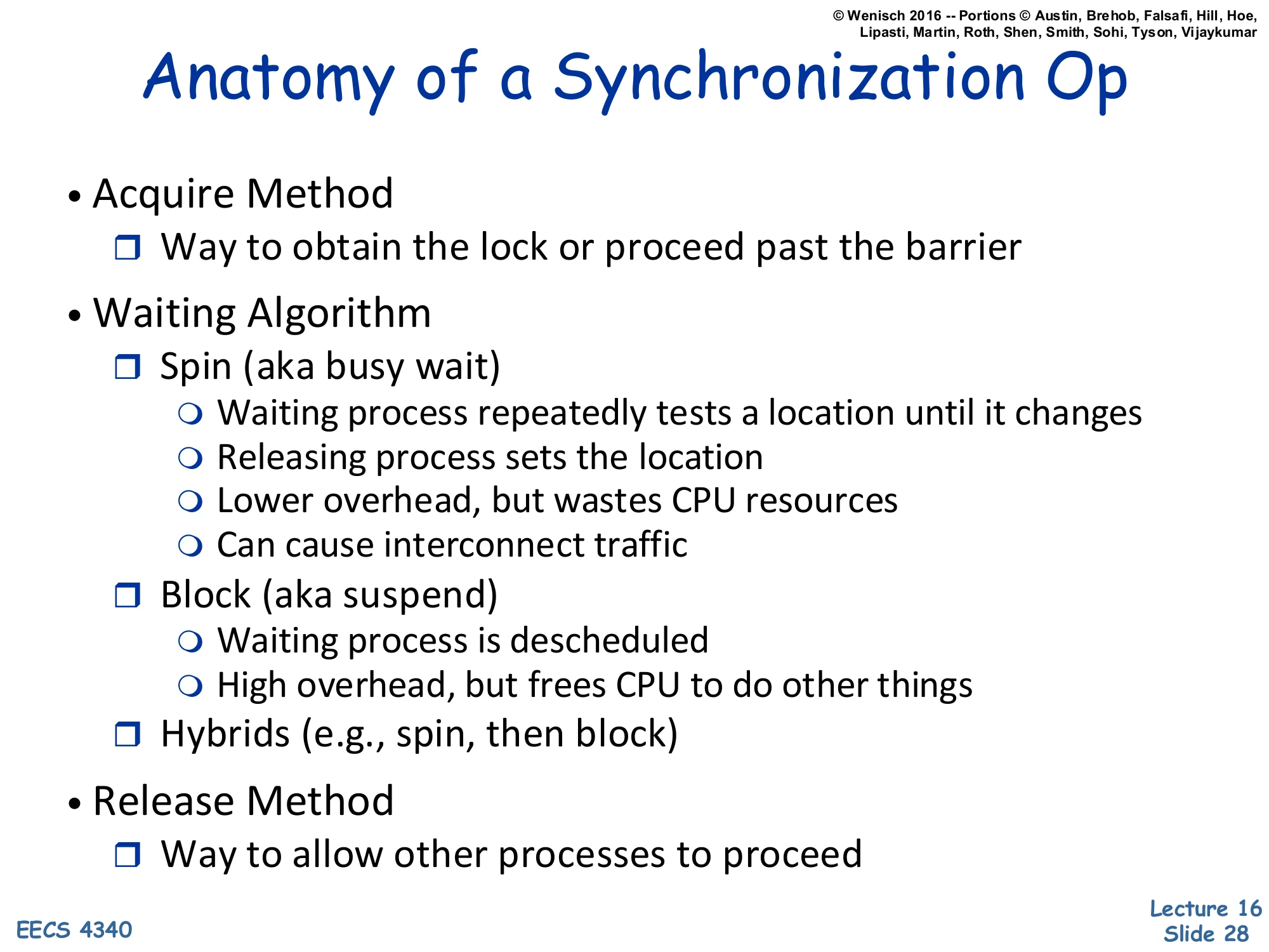
- Acquire Method
- Way to obtain the lock or proceed past the barrier
- Waiting Algorithm
- Spin (aka busy wait)
- Waiting process repeatedly tests a location until it changes
- Releasing process sets the location
- Lower overhead, but wastes CPU resources
- Can cause interconnect traffic
- Block (aka suspend)
- Waiting process is descheduled
- High overhead, but frees CPU to do other things
- Hybrids (e.g., spin, then block)
- Spin (aka busy wait)
- Release Method
- Way to allow other processes to proceed
A synchronization operation decomposes into three pieces. The acquire obtains the resource — testing and setting a lock variable, decrementing a barrier count, popping a queue. The waiting algorithm governs what to do when acquire fails because the resource is held. Spin-waiting busy-loops on a memory location; the latency is just the load-to-load gap, but the spinning thread occupies a core and can flood the interconnect with coherence traffic. Block-waiting parks the thread (e.g., futex_wait or a kernel semaphore); the latency includes a context switch (microseconds), but the CPU is free for other work. Hybrid (adaptive) strategies spin briefly then block — appropriate when expected wait times are short but variable. Finally, release makes the resource available again, often by storing a sentinel value or signaling waiters. Each piece interacts with the coherence protocol: a spin-loop that hammers an exclusively-held cache line generates pathological invalidate traffic, motivating test-and-test-and-set and MCS locks.
HW/SW Implementation Trade-offs
Show slide text
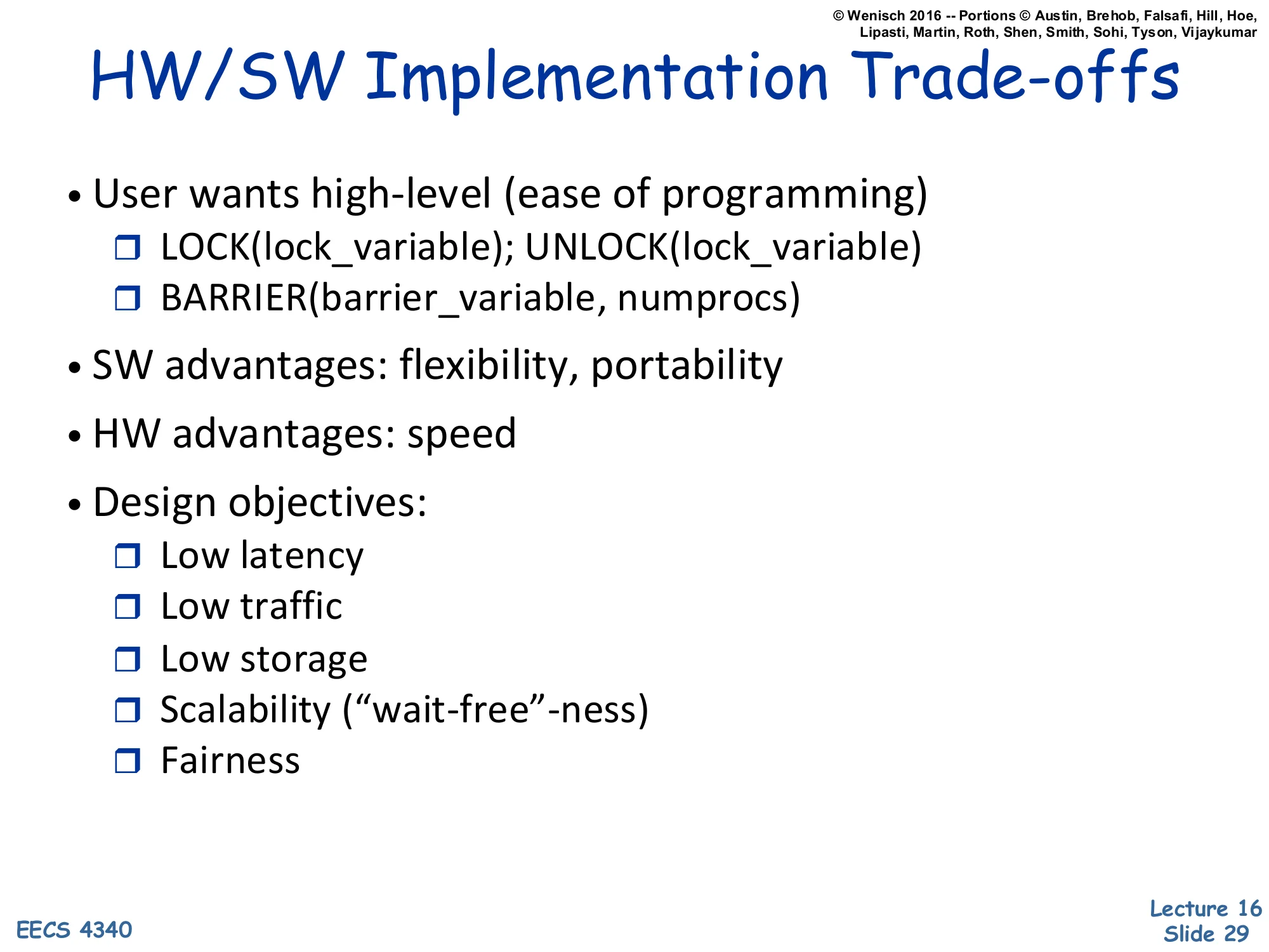
HW/SW Implementation Trade-offs
- User wants high-level (ease of programming)
- LOCK(lock_variable); UNLOCK(lock_variable)
- BARRIER(barrier_variable, numprocs)
- SW advantages: flexibility, portability
- HW advantages: speed
- Design objectives:
- Low latency
- Low traffic
- Low storage
- Scalability (“wait-free”-ness)
- Fairness
The user-visible API is small: LOCK(L), UNLOCK(L), BARRIER(B, n). The implementation can sit anywhere on a HW/SW spectrum. Pure software implementations (Peterson’s algorithm, ticket locks) need only ordinary loads and stores plus a memory model — they’re maximally portable but slow under contention. Hardware-assisted primitives (LL/SC, CAS, atomic FAA) reduce the round-trip to a single instruction but require ISA support. Pure hardware locks (Cray T3D’s atomic-swap unit) bypass coherence entirely — fast but inflexible. Five design objectives compete: latency (uncontended cost), traffic (interconnect bandwidth under contention), storage (per-lock overhead), scalability — sometimes phrased as ‘wait-freedom’, meaning every thread completes in bounded steps regardless of others — and fairness (no starvation). MCS locks score well on traffic and fairness; ticket locks on fairness; spinlocks on latency; transactional memory on scalability when contention is rare. No primitive wins on all axes.
Synchronization Challenges
Show slide text
Challenges
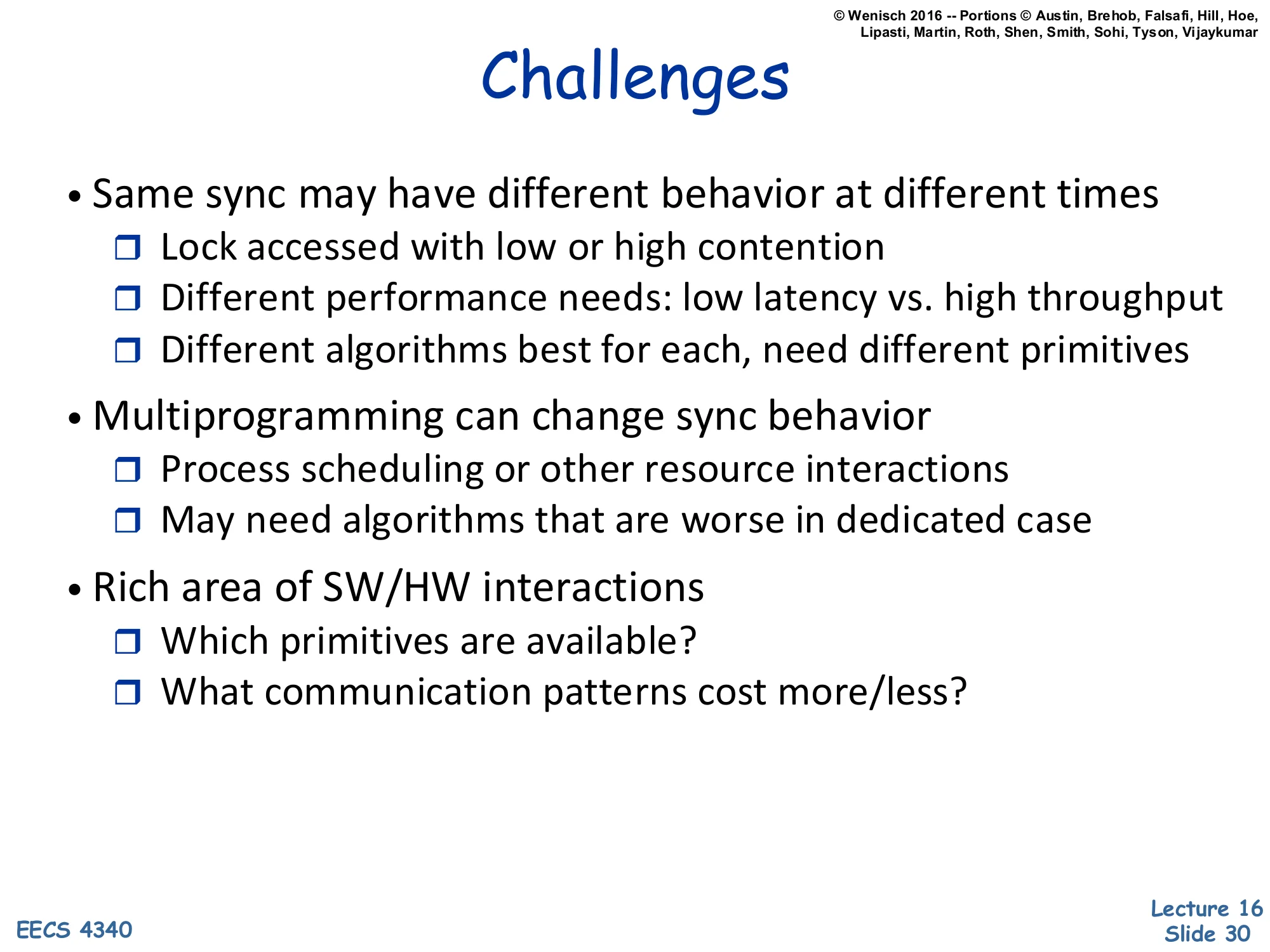
- Same sync may have different behavior at different times
- Lock accessed with low or high contention
- Different performance needs: low latency vs. high throughput
- Different algorithms best for each, need different primitives
- Multiprogramming can change sync behavior
- Process scheduling or other resource interactions
- May need algorithms that are worse in dedicated case
- Rich area of SW/HW interactions
- Which primitives are available?
- What communication patterns cost more/less?
The synchronization landscape is hard partly because the same lock can have wildly different behavior over time. Under low contention, you want minimal latency: a simple test-and-set is fine. Under high contention, you want to avoid the cache-line ping-pong of test-and-set and instead use a back-off scheme, a queue lock, or even adaptive blocking. Multiprogramming — multiple unrelated processes sharing a core — makes things worse because the OS scheduler may deschedule the lock holder, leading to convoy effects where many waiters spin uselessly. Robust algorithms must handle both dedicated and time-shared cases, sometimes with measurably worse dedicated-case performance. The HW/SW co-design here is rich: how expensive is a cache line invalidation? Does the ISA expose atomic primitives? Can the OS yield to a lock holder? These questions repeat in every coherence/consistency lecture.
Coherency and Consistency
Cache Coherence — Two ATMs Example
Show slide text
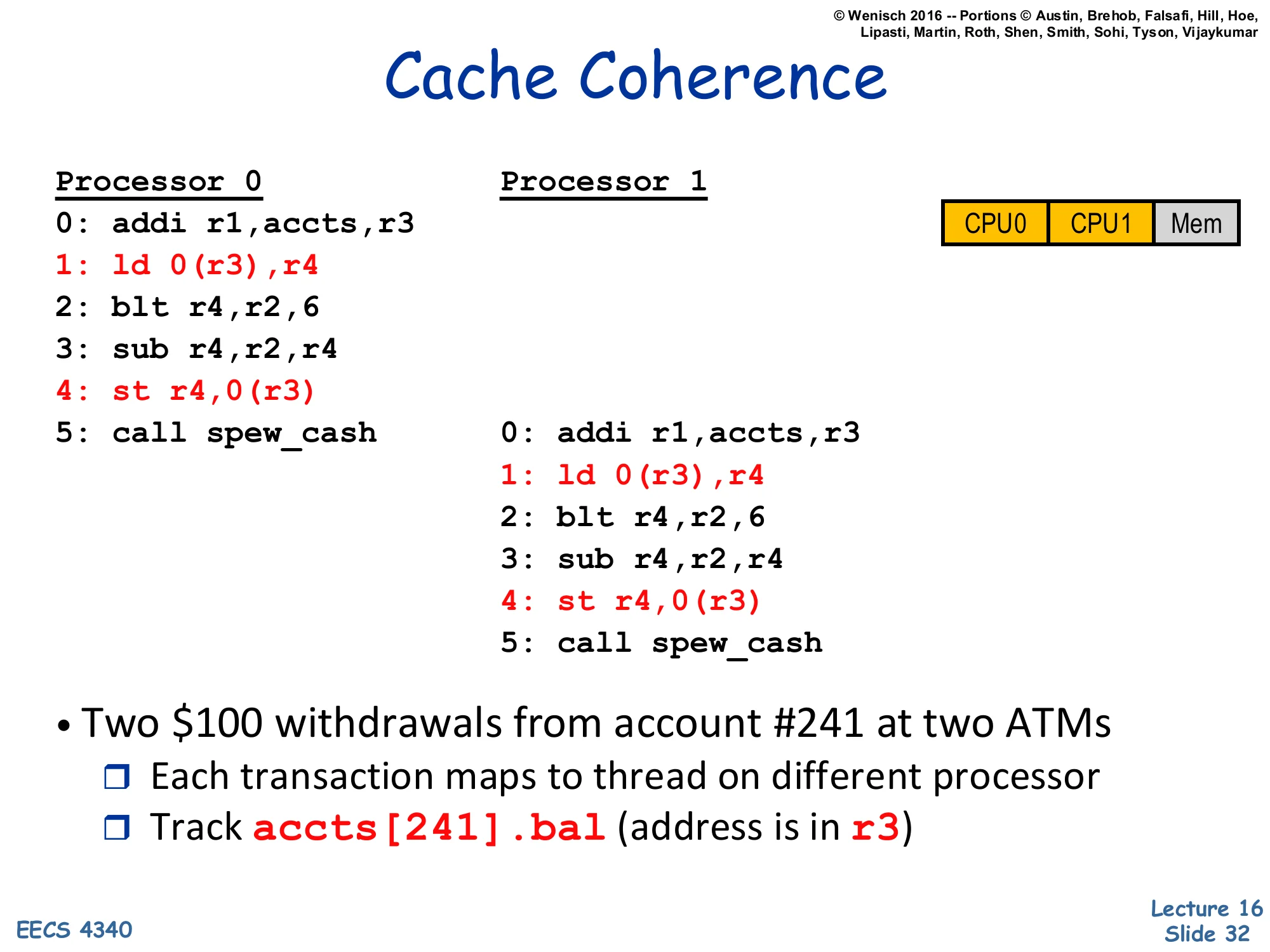
Cache Coherence
Processor 0 Processor 10: addi r1,accts,r31: ld 0(r3),r42: blt r4,r2,63: sub r4,r2,r44: st r4,0(r3)5: call spew_cash 0: addi r1,accts,r3 1: ld 0(r3),r4 2: blt r4,r2,6 3: sub r4,r2,r4 4: st r4,0(r3) 5: call spew_cashDiagram: CPU0 | CPU1 | Mem
- Two $100 withdrawals from account #241 at two ATMs
- Each transaction maps to thread on different processor
- Track
accts[241].bal(address is inr3)
This canonical example sets up the coherence problem with a real-world hook. Two ATMs simultaneously process $100 withdrawals from account #241. Each ATM’s transaction runs as a thread on a different processor. The code reads the current balance into r4, checks that it’s at least the withdrawal amount (blt), subtracts and writes back, then logs the transaction (call spew_cash). The balance variable accts[241].bal lives at memory address (r3). The next two slides show what happens with and without caches. Without coherence, you can get the classical ‘lost update’ bug where both ATMs read the original $500, both subtract $100 to get $400, and both write $400 back — the bank loses $100. The lecture walks through this in detail to motivate hardware-managed coherence.
No-Cache, No-Problem
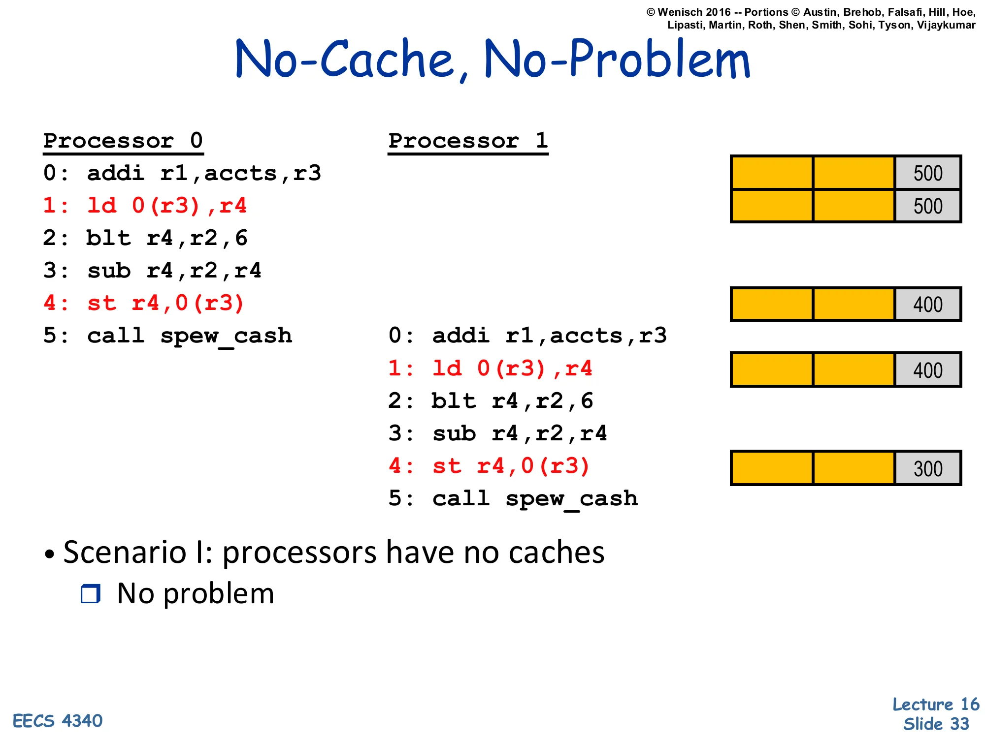
Show slide text
No-Cache, No-Problem
Processor 0 Processor 10: addi r1,accts,r3 Mem 5001: ld 0(r3),r4 Mem 5002: blt r4,r2,63: sub r4,r2,r44: st r4,0(r3) Mem 4005: call spew_cash 0: addi r1,accts,r3 1: ld 0(r3),r4 Mem 400 2: blt r4,r2,6 3: sub r4,r2,r4 4: st r4,0(r3) Mem 300 5: call spew_cash- Scenario I: processors have no caches
- No problem
Without caches, each load and store goes directly to main memory, which serializes all accesses on a single bus or memory controller. Processor 0 loads 500 from memory, computes 400, stores 400 back. Processor 1 then loads 400 (the value P0 just stored), computes 300, stores 300. The final balance is correct: 300. The serialization point — main memory — provides a global order on accesses, which is exactly what consistency demands. The cost, of course, is that every load and every store hits main memory, so there’s no latency hiding and the memory bandwidth is shared by every access. In real machines, this is unworkable: caches reduce average memory latency by 10–100×. So we get caches, but caches reintroduce the problem the next slide describes.
Cache Incoherence
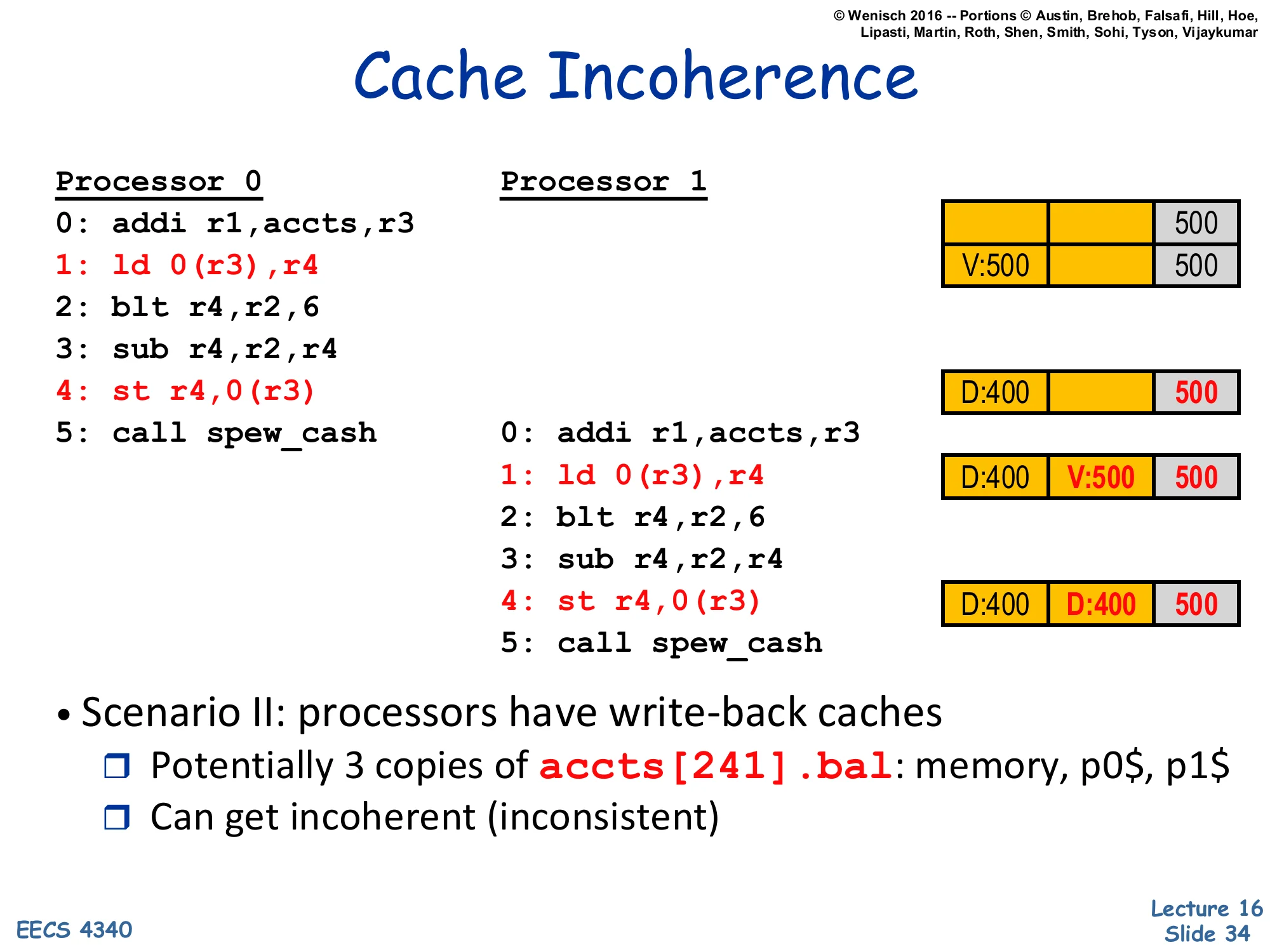
Show slide text
Cache Incoherence
Processor 0 Processor 1 P0$ P1$ Mem0: addi r1,accts,r3 5001: ld 0(r3),r4 V:500 5002: blt r4,r2,63: sub r4,r2,r44: st r4,0(r3) D:400 5005: call spew_cash 0: addi r1,accts,r3 1: ld 0(r3),r4 D:400 V:500 500 2: blt r4,r2,6 3: sub r4,r2,r4 4: st r4,0(r3) D:400 D:400 500 5: call spew_cash- Scenario II: processors have write-back caches
- Potentially 3 copies of
accts[241].bal: memory, p0$, p1$ - Can get incoherent (inconsistent)
- Potentially 3 copies of
With per-CPU write-back caches and no coherence protocol, the example breaks. P0 loads, gets 500 from memory, stores 500 cached as Valid. P0 then writes 400 — its cache transitions to Dirty (D:400), but main memory still holds 500. P1 now loads — but P1’s cache misses, fetches from main memory (which has the stale 500), and gets 500. Both caches have different valid values; P1 then writes 300 (D:300 in its cache). The final state shows two dirty cache lines with different values (P0$=400, P1$=400 in this trace, but the value depends on interleaving) plus an out-of-date memory. When the dirty lines eventually evict, whichever one writes back last wins, and the other update is silently lost. This is cache incoherence: multiple cached copies of one address holding inconsistent values. The fix — snooping or directory protocols — is the next 14 slides.
Snooping Cache-Coherence Protocols
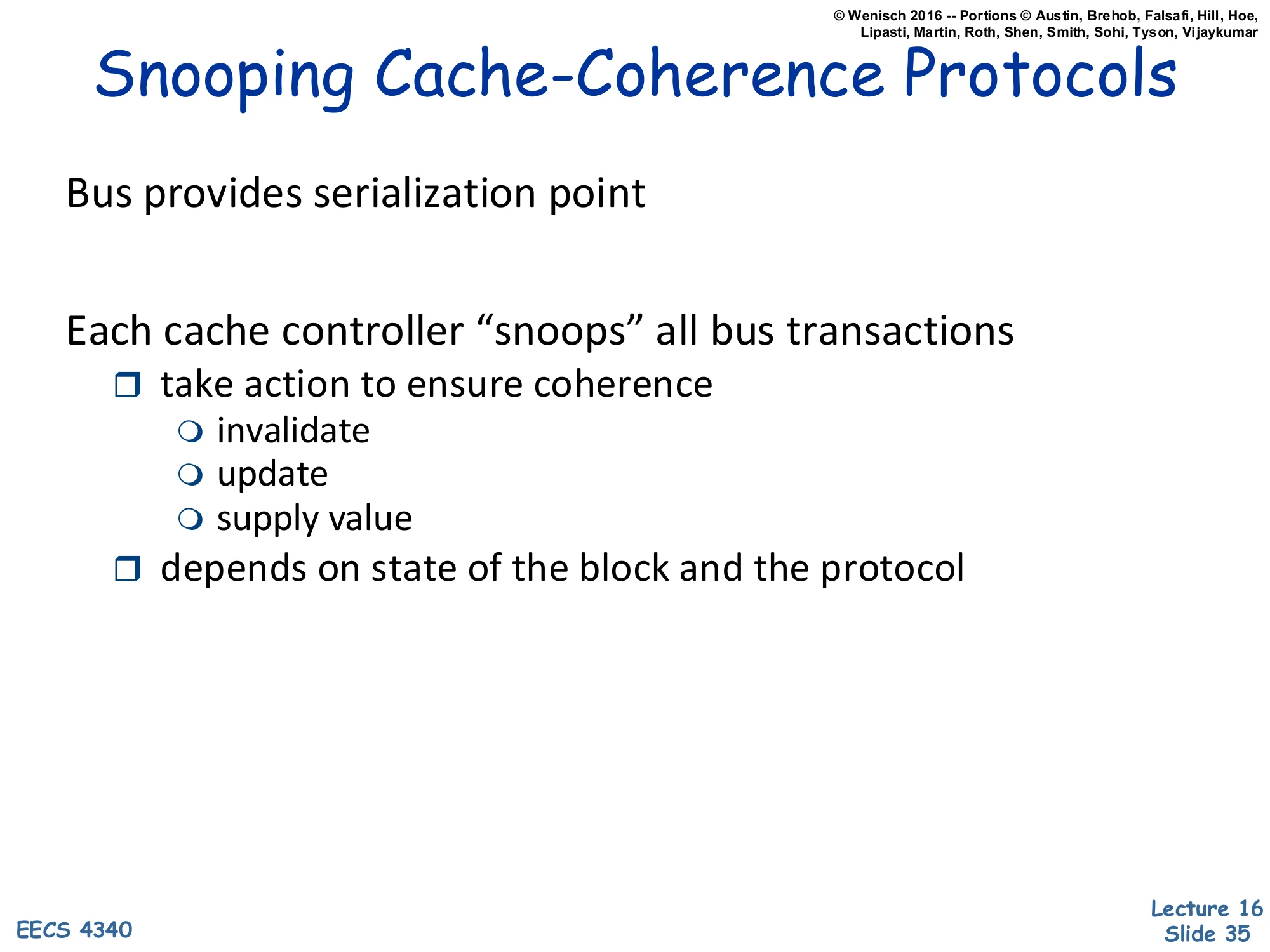
Show slide text
Snooping Cache-Coherence Protocols
Bus provides serialization point
Each cache controller “snoops” all bus transactions
- take action to ensure coherence
- invalidate
- update
- supply value
- depends on state of the block and the protocol
Snooping coherence is the simplest hardware coherence model and is the one used in classical bus-based SMPs and small CMPs. The shared bus serves as a serialization point: every cache miss broadcasts a request on the bus, and the bus decides a global order on these transactions. Each cache controller listens (snoops) on the bus continuously. When it sees a request relevant to a line it caches, it reacts: invalidate its copy if another cache asks to write the line; supply the line if another cache asks to read it and we hold the only modified copy; update its copy in some protocol variants. The reaction depends on the line’s local state (Modified, Shared, Invalid in MSI; +Exclusive in MESI) and the bus message (BusRd, BusRdX, BusInv). Snooping doesn’t scale beyond ~16 cores because every core must snoop every bus transaction, but it’s elegant and small.
Scalable Cache Coherence
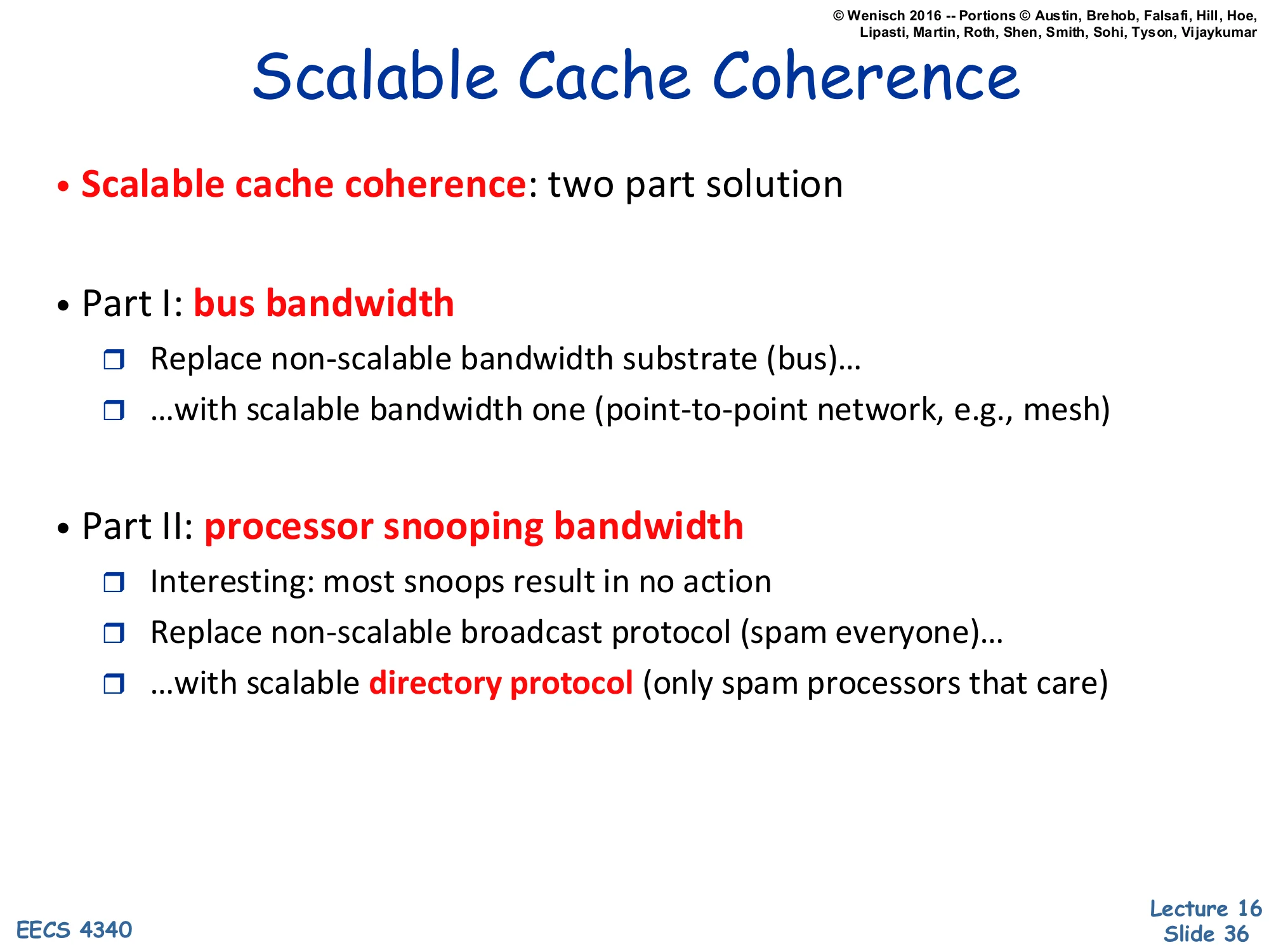
Show slide text
Scalable Cache Coherence
- Scalable cache coherence: two part solution
- Part I: bus bandwidth
- Replace non-scalable bandwidth substrate (bus)…
- …with scalable bandwidth one (point-to-point network, e.g., mesh)
- Part II: processor snooping bandwidth
- Interesting: most snoops result in no action
- Replace non-scalable broadcast protocol (spam everyone)…
- …with scalable directory protocol (only spam processors that care)
Scaling snooping coherence beyond a handful of cores requires fixing two bottlenecks. Bus bandwidth is the obvious one: a single shared bus saturates as cores are added, so it must be replaced with a point-to-point network — a 2D mesh, ring, or crossbar — whose bisection bandwidth grows with size. But there’s a second, less obvious bottleneck: snoop bandwidth at each cache. Even if the network can carry more traffic, every snoop request still has to be tag-checked at every cache, and most of those checks return ‘no, I don’t have this line’. The fix is the directory protocol: a directory at the home node tracks which caches actually share each line, and the protocol sends point-to-point messages only to those caches. Snoop bandwidth scales linearly per node instead of with the system’s total miss rate. This is the architectural pivot from SMPs to NUMA/directory machines like the SGI Origin and modern 50+-core processors.
Approaches to Cache Coherence
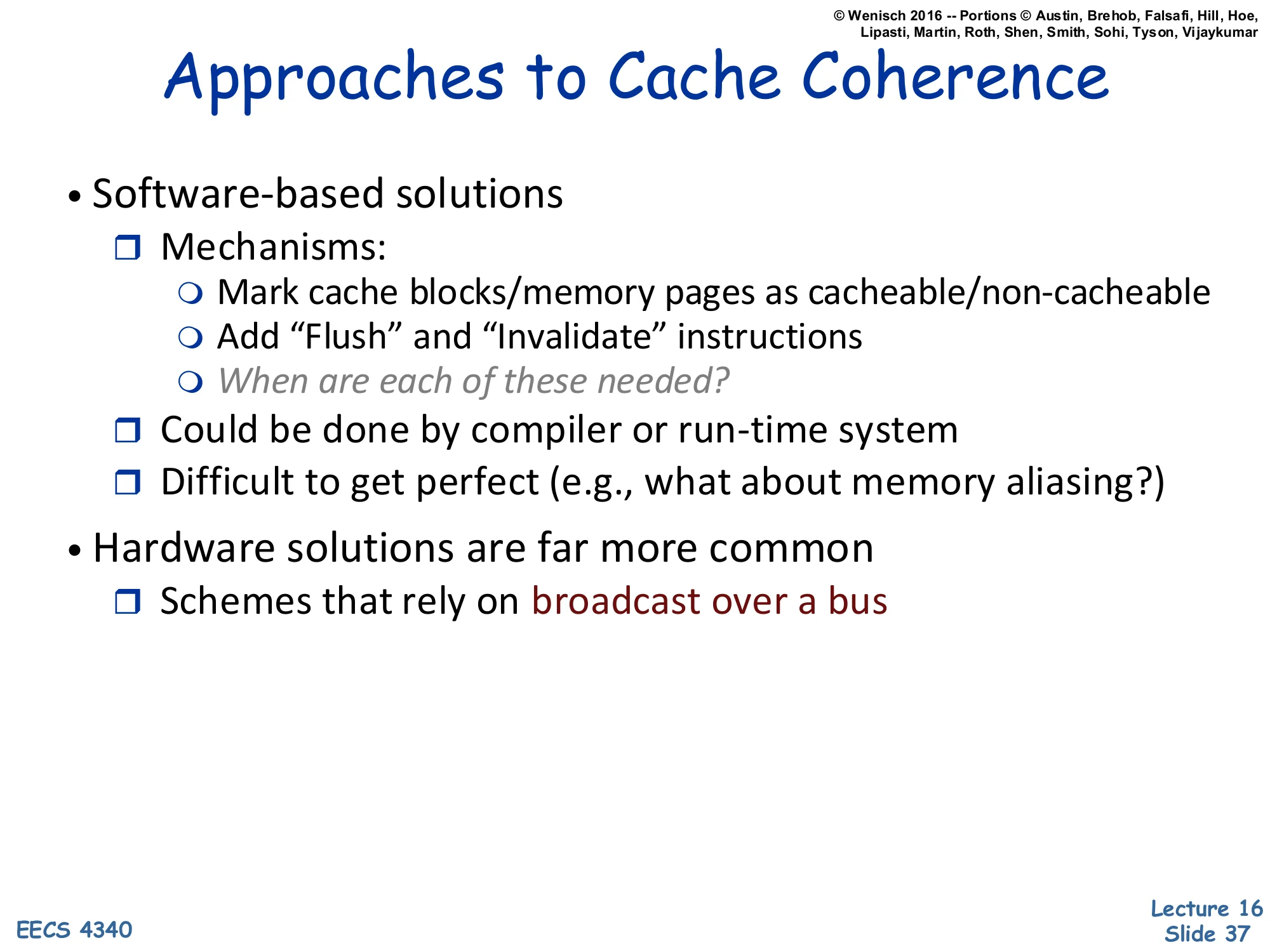
Show slide text
Approaches to Cache Coherence
- Software-based solutions
- Mechanisms:
- Mark cache blocks/memory pages as cacheable/non-cacheable
- Add “Flush” and “Invalidate” instructions
- When are each of these needed?
- Could be done by compiler or run-time system
- Difficult to get perfect (e.g., what about memory aliasing?)
- Mechanisms:
- Hardware solutions are far more common
- Schemes that rely on broadcast over a bus
Coherence can in principle be enforced by software: mark shared pages as non-cacheable so every access goes to memory, or insert flush and invalidate instructions at synchronization points to push dirty cached data to memory and discard stale lines before reading. Some early machines and many embedded systems still rely on these. Compiler or runtime systems could in principle do it automatically — but determining when a flush or invalidate is needed requires precise alias analysis and inter-procedural reasoning that, in general, is undecidable. The ‘memory aliasing’ caveat is the killer: pointer aliasing makes it impossible to know statically whether two pointers refer to the same line. Hardware coherence protocols sidestep all of this by using cache state machines that conservatively track which lines might be shared. Hardware coherence is now ubiquitous in general-purpose chips; software coherence persists only in specialized contexts (some GPU shared memory, scratchpad architectures).
Valid-Invalid Snooping Protocol
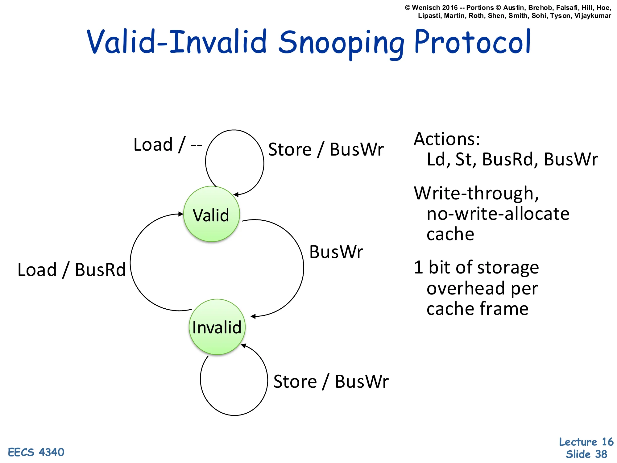
Show slide text
Valid-Invalid Snooping Protocol
State machine with two states, Valid and Invalid.
- Valid → Valid on Load / —
- Valid → Valid on Store / BusWr
- Valid → Invalid on BusWr (snoop)
- Invalid → Valid on Load / BusRd
- Invalid → Invalid on Store / BusWr
Actions: Ld, St, BusRd, BusWr
Write-through, no-write-allocate cache
1 bit of storage overhead per cache frame
The simplest hardware coherence protocol has just two states, mirroring an ordinary cache valid bit. Valid means we hold a clean copy; Invalid means we don’t. Loads succeed if Valid; on Invalid, fetch via BusRd. Every store goes to the bus as BusWr (write-through semantics) — this both updates main memory and tells other caches to invalidate their copies (the snoop on BusWr transitions other caches from Valid to Invalid). The protocol works because: (1) writes are always serialized on the bus; (2) once invalidated, a cache must refetch on the next read. The cost is that every store generates bus traffic, even repeated stores to the same line — that’s the price of write-through and the absence of a Modified state. Two-state protocols are simple to verify but unacceptable for performance; the next slide upgrades to three-state MSI.
MSI Protocol — States and Messages
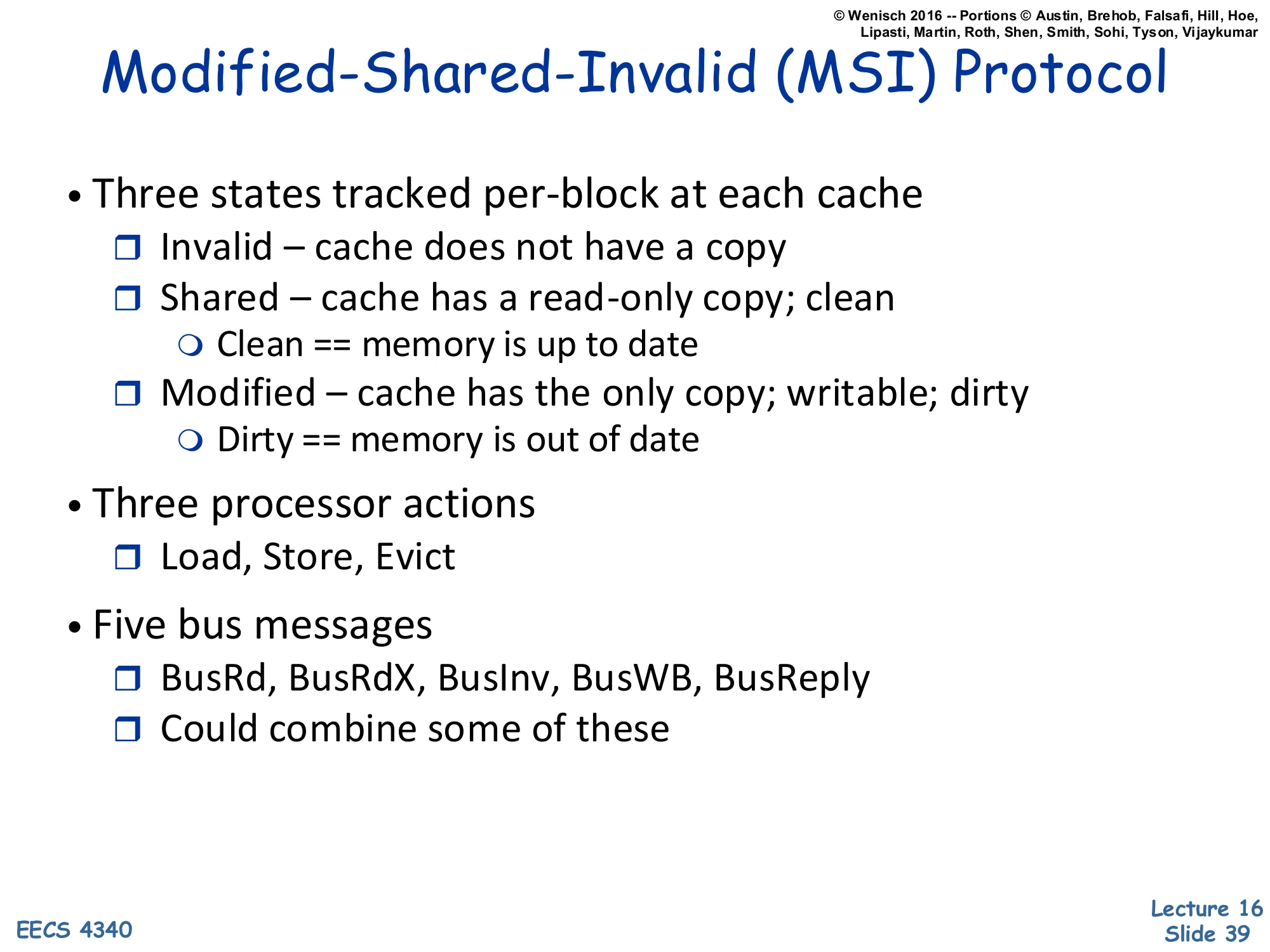
Show slide text
Modified-Shared-Invalid (MSI) Protocol
- Three states tracked per-block at each cache
- Invalid – cache does not have a copy
- Shared – cache has a read-only copy; clean
- Clean == memory is up to date
- Modified – cache has the only copy; writable; dirty
- Dirty == memory is out of date
- Three processor actions
- Load, Store, Evict
- Five bus messages
- BusRd, BusRdX, BusInv, BusWB, BusReply
- Could combine some of these
The MSI protocol is the canonical write-back coherence protocol and the foundation for MESI and MOESI. Three states: Invalid (cache doesn’t have it), Shared (clean read-only copy, others may also share, memory is up to date), Modified (dirty exclusive copy, this cache is the only one with valid data, memory is stale). Three processor actions trigger transitions: Load (read), Store (write), Evict (replace this line). Five bus messages: BusRd asks for read access; BusRdX asks for read-exclusive (intent to write, so other copies must invalidate); BusInv asks others to invalidate without fetching data (used when upgrading from S to M); BusWB writes a dirty line back to memory; BusReply is a data response. Real protocols combine some — e.g., BusRdX and BusInv can fold together — but five is the textbook count. The next several slides build the state machine incrementally.
MSI Protocol — Invalid → Shared on Load
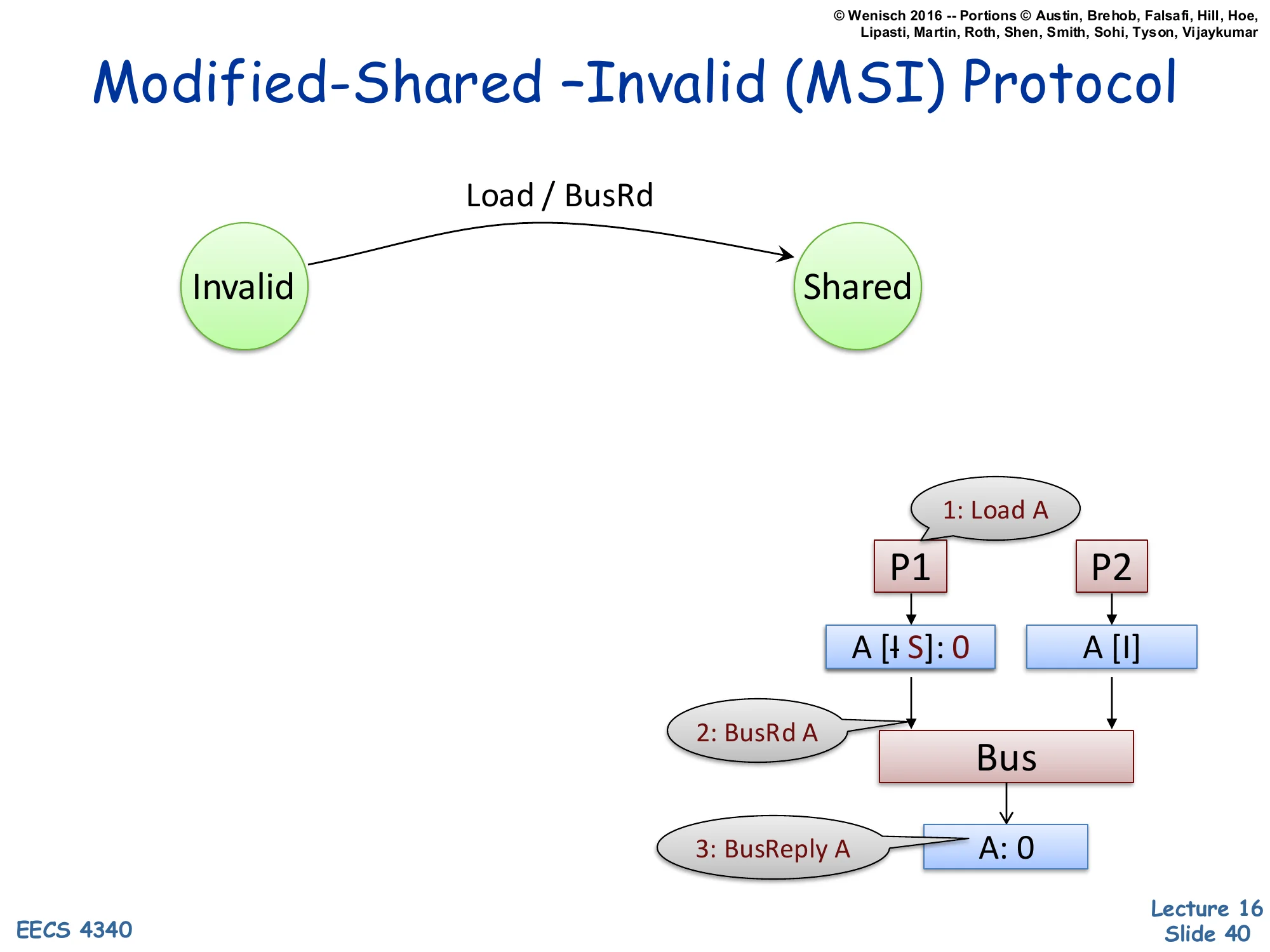
Show slide text
Modified-Shared –Invalid (MSI) Protocol
State transition: Invalid → Shared on Load / BusRd.
Example trace:
1: Load AP1 ────────► ▼ A [I→S]: 0 A [I] │ │ ▼ ▼ 2: BusRd A Bus │ ▼ 3: BusReply A A: 0The first transition adds the Invalid → Shared edge triggered by a processor Load. P1 wants to load address A; its local cache is Invalid (cache miss). P1 issues BusRd A on the bus (step 2). Memory replies with the data (step 3, BusReply A: 0). P1’s cache transitions to Shared, holding the value 0. P2’s cache (also Invalid) snoops the BusRd but ignores it because it has no copy of A. The convention A [I→S]: 0 means the line for A transitions from I to S with current value 0. The crossed-out ‘I’ visualization in the slide indicates the prior state. This is the simplest case: one reader, no writers, no contention. The next slides add a second reader, an evict, and finally a writer to build out the full protocol.
MSI Protocol — Adding BusRd Snoop in Shared
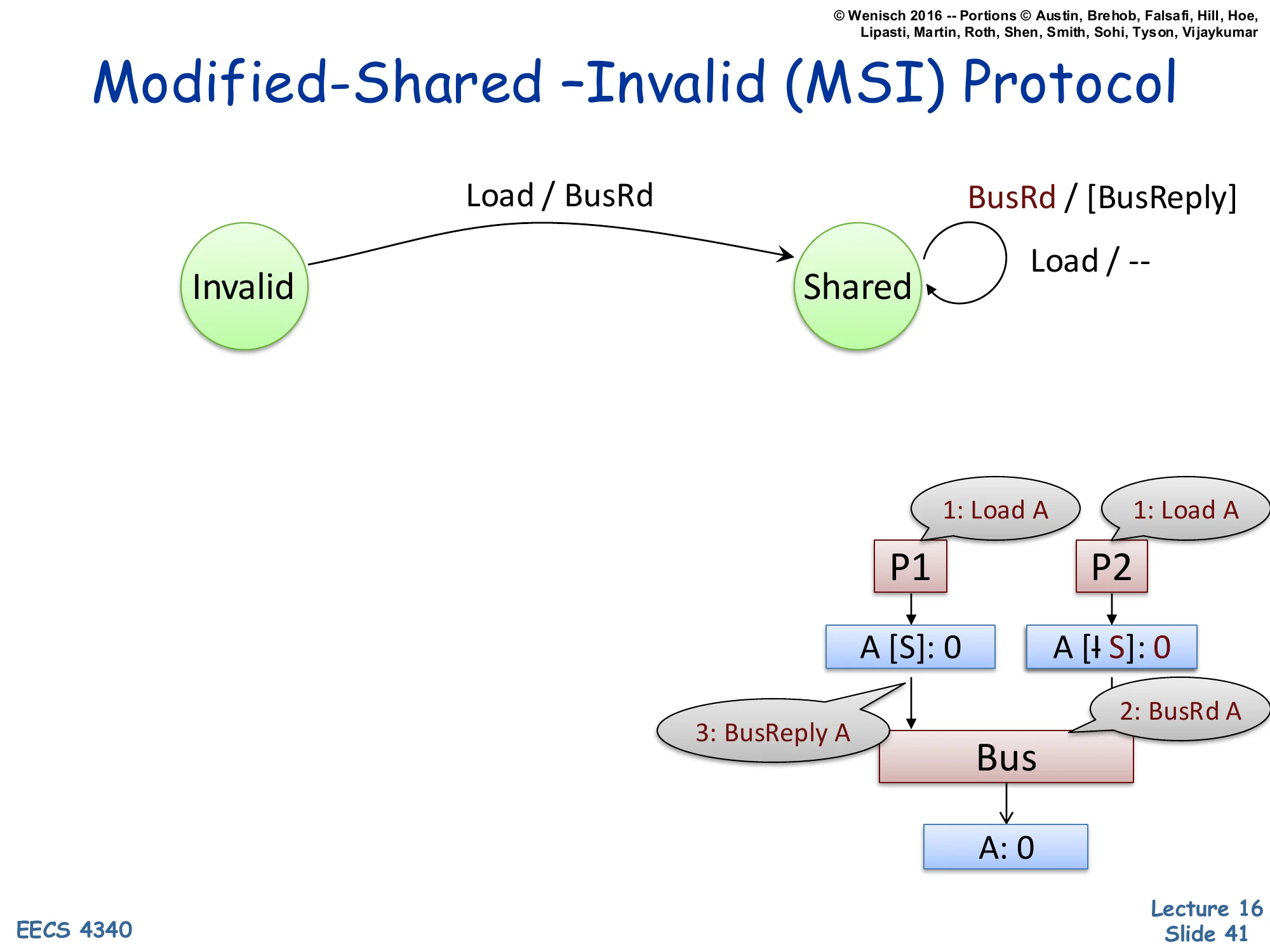
Show slide text
Modified-Shared –Invalid (MSI) Protocol
New transitions:
- Invalid → Shared on Load / BusRd
- Self-loop on Shared: Load / — (silent), and BusRd / [BusReply] (supply data)
Example trace:
1: Load A 1: Load A ▼ ▼ A [S]: 0 A [I→S]: 0 │ │ │ 3: BusReply A │ 2: BusRd A └──────► Bus ◄─────┘ │ ▼ A: 0Now P1 already holds A in Shared (from the previous slide). P2 issues a Load that misses, sends BusRd A on the bus. Two new transitions appear: a self-loop on Shared for processor Load (action: nothing — a hit, no bus traffic), and a self-loop on Shared for snooped BusRd (action: optionally supply the data via BusReply A — known as cache-to-cache transfer). Whether the supplier is the holding cache or main memory depends on the implementation; either is correct because in Shared, the cached value matches memory (‘clean’). P2’s cache transitions Invalid → Shared, ending with both caches holding A in Shared and the same value. The key correctness property: while a line is in Shared, all valid copies hold the same value as memory. Multiple readers, no writers — the read-shared common case for shared data.
MSI Protocol — Evict from Shared
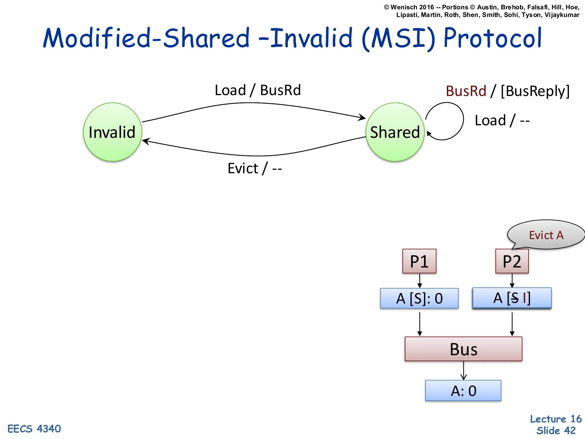
Show slide text
Modified-Shared –Invalid (MSI) Protocol
New transition: Shared → Invalid on Evict / — (silent eviction, no bus traffic).
Example trace: P2 evicts its copy of A locally; no bus message needed because A was clean.
Evict AP1 P2 ▼ ▼ A [S]: 0 A [S→I]When a line in Shared is evicted (e.g., due to a capacity miss replacing it), the protocol is allowed to drop it silently — no bus traffic. This is correct because Shared means the line is clean (matches memory), so there is no data loss in discarding it. P2’s cache transitions Shared → Invalid; P1 still holds A in Shared. Note the asymmetry with Modified evictions: a dirty Modified line cannot be silently dropped — it must be written back to memory via BusWB before transitioning to Invalid (slide 47). Silent S→I eviction is critical for performance: the bulk of cache evictions happen on read-mostly data, so making them traffic-free saves significant bus bandwidth. Some advanced protocols (like MESIF) also add Forward state to designate a single ‘responder’ for shared lines, optimizing the cache-to-cache transfer of slide 41.
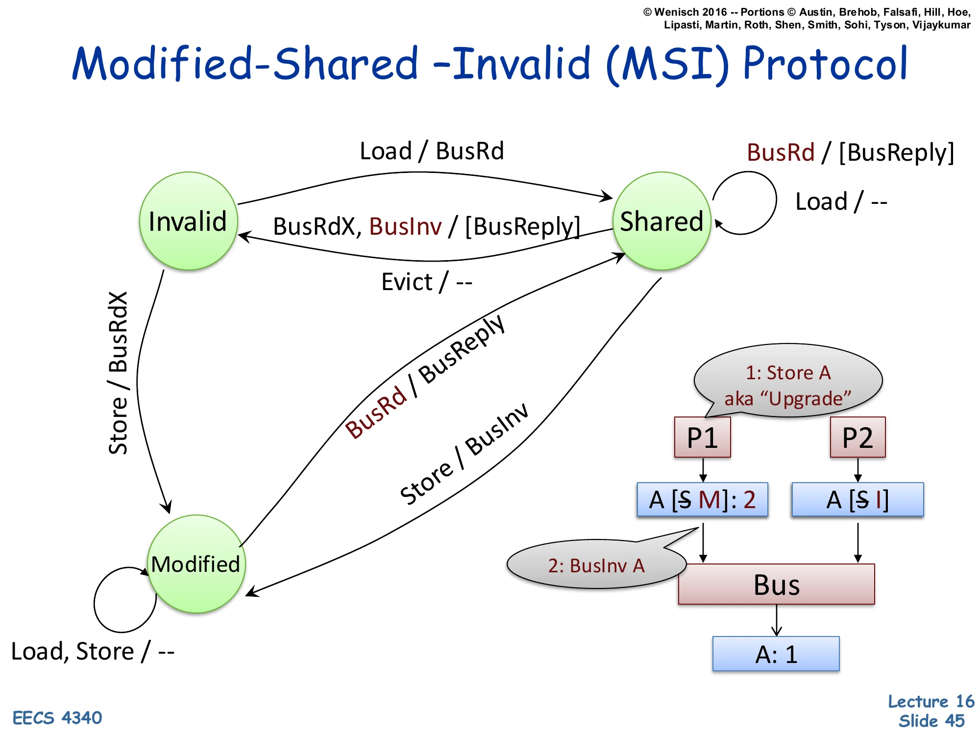
MSI Protocol — Invalid → Modified on Store
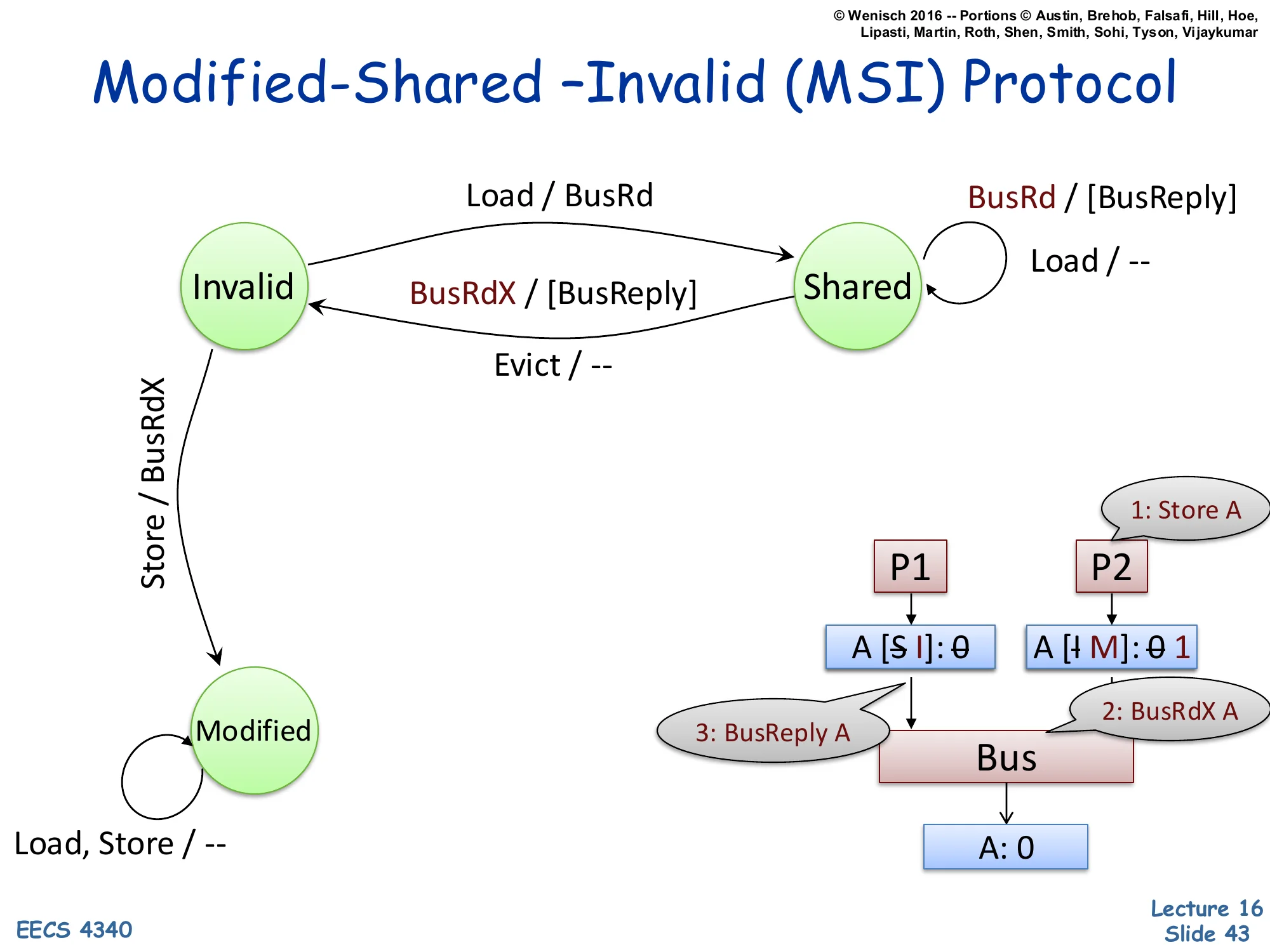
Show slide text
Modified-Shared –Invalid (MSI) Protocol
New transitions:
- Invalid → Modified on Store / BusRdX
- Self-loop on Modified: Load, Store / —
- Shared → Invalid on snooped BusRdX / [BusReply]
Example trace:
1: Store A P2 wants to write ▼ A [S→I]: 0 A [I→M]: 0→1 │ │ │ 3: BusReply │ 2: BusRdX A └────► Bus ◄───┘ │ ▼ A: 0Now we add a writer. P2 issues a Store to A; its cache is Invalid. To store, P2 needs exclusive access, so it issues BusRdX A (read-exclusive). P1’s cache, holding A in Shared, snoops BusRdX and must transition Shared → Invalid, optionally supplying the current data via BusReply (so the requester gets the latest value before writing). P2’s cache transitions Invalid → Modified with the new value 1. The Modified self-loop says: while in Modified, future Loads and Stores by this processor are local hits with no bus traffic — this is the major performance win of write-back over write-through. Every bus transaction costs cycles and energy; once a line is privately Modified, repeated writes are essentially free. Modified ⇔ exclusive ⇔ memory-is-stale; only the holding cache has the truth.
MSI Protocol — Modified → Shared on Snoop BusRd
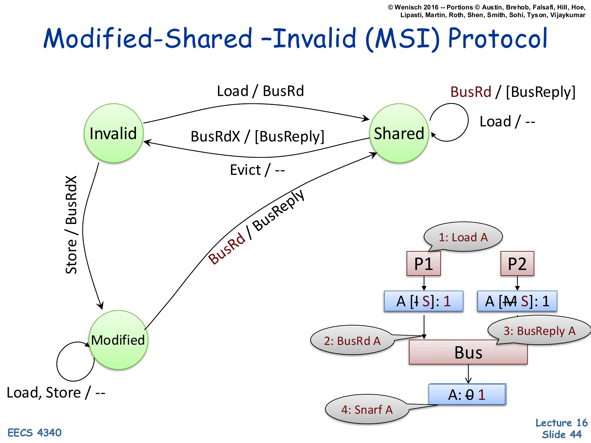
Show slide text
Modified-Shared –Invalid (MSI) Protocol
New transition: Modified → Shared on snooped BusRd / BusReply (supply value, downgrade).
Example trace:
1: Load A (other CPU) ▼ ▼ A [I→S]: 1 A [M→S]: 1 │ │ │ 2: BusRd A │ 3: BusReply A └────► Bus ◄───┘ │ ▼ A: 0→1 (4: Snarf A, memory updates)Now the symmetric case: a reader arrives at a line another cache holds in Modified. P2 holds A in Modified with value 1 (memory still has 0). P1 issues a Load, misses, sends BusRd A. P2 snoops BusRd, recognizes it has the only valid copy, and supplies the data via BusReply (cache-to-cache transfer). Critically, P2 must also downgrade Modified → Shared because there are now two readers. Memory snarfs the value off the bus during the BusReply, updating itself from 0 to 1 — this is necessary so that future BusRd from a third reader can be satisfied by memory (which is now back in sync). P1 ends in Shared with value 1; P2 downgraded to Shared with value 1; memory holds 1. Observation: the transition from M→S is forced by the protocol invariant that Shared implies clean — so memory must catch up before anyone else can share.
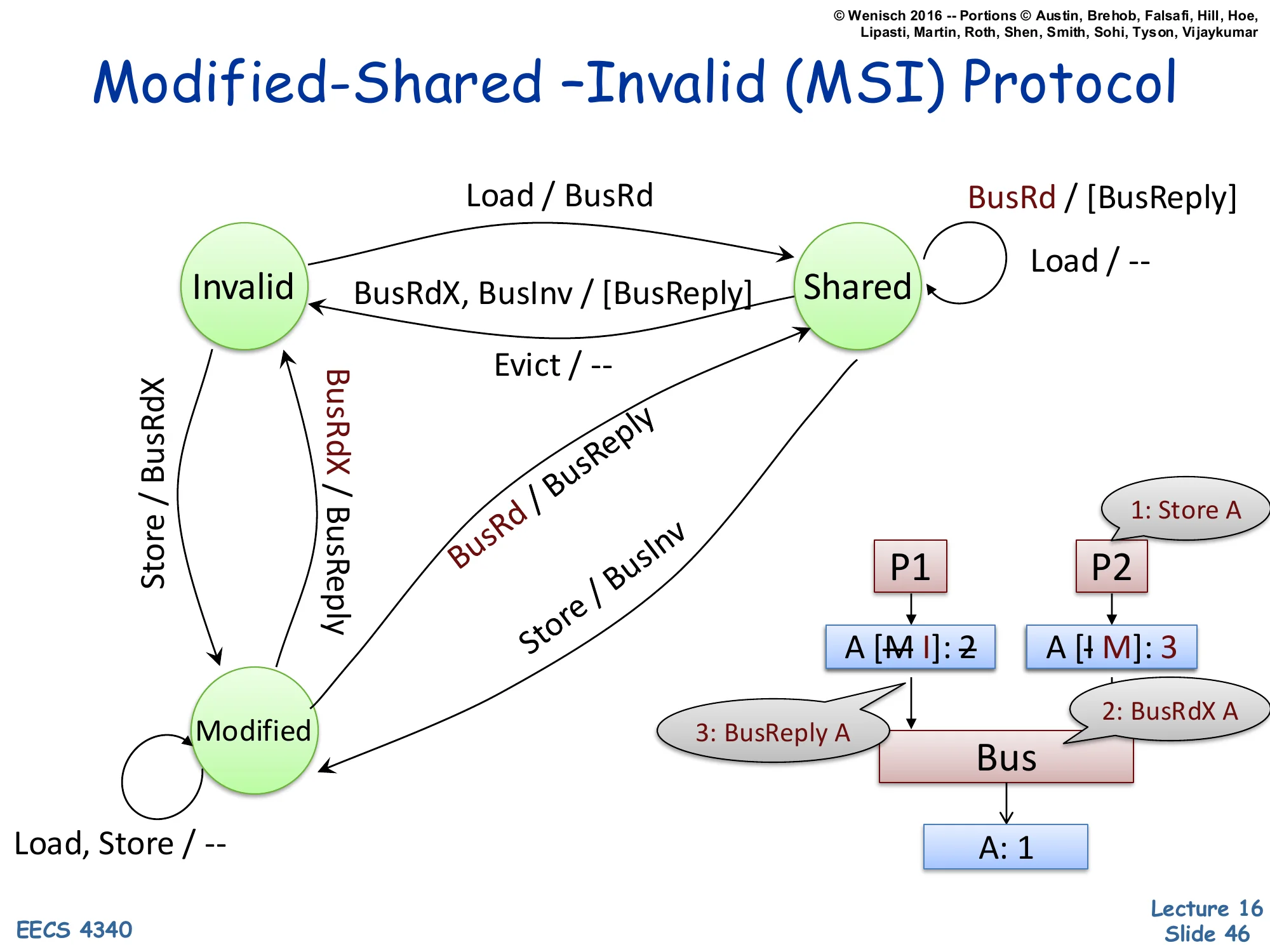
MSI Protocol — Shared → Modified on Store (Upgrade)
Show slide text
Modified-Shared –Invalid (MSI) Protocol
New transitions:
- Shared → Modified on Store / BusInv
- Snooped BusInv in Shared → Invalid (no data reply needed)
Example trace: 1: Store A aka "Upgrade"
P1 (writer) P2 ▼ ▼ A [S→M]: 2 A [S→I] │ │ │ 2: BusInv A │ └────────────► Bus ◄─────────┘ │ ▼ A: 1When P1 already holds A in Shared and wants to write, it doesn’t need to fetch the data — it already has it. It only needs to invalidate the other sharers. The optimization is the BusInv (or ‘Upgrade’) message: a bus request that says ‘I’m taking this line exclusively; everyone else, drop it.’ P1 transitions Shared → Modified, P2 transitions Shared → Invalid (no BusReply data needed since P1 already has the current clean value). This saves a data transfer compared to BusRdX. The aka ‘Upgrade’ annotation captures the semantic: this is a state upgrade (S → M) without a data fetch. Implementations typically combine BusRdX and BusInv into a single ‘GetX’ message that signals ‘I want this line exclusive’, with an optional data flag.
MSI Protocol — Modified → Invalid on Snoop BusRdX
Show slide text
Modified-Shared –Invalid (MSI) Protocol
New transition: Modified → Invalid on snooped BusRdX / BusReply (supply data + invalidate).
Example trace:
(other writer) 1: Store A ▼ ▼ A [M→I]: 2 A [I→M]: 3 │ │ │ 3: BusReply A │ 2: BusRdX A └────────► Bus ◄─────┘ │ ▼ A: 1The case where both processors are writers. P2 (or another core) currently holds A in Modified with value 2 — memory has stale value 1. P1 wants to write a new value 3. P1 issues BusRdX A. P2 snoops BusRdX, must give up its Modified copy: it sends BusReply A with current value 2 (so P1 sees the latest data before writing 3 over it), then transitions Modified → Invalid. P1’s cache transitions Invalid → Modified with value 3. After this transaction, only P1 holds A; memory still has stale data, which is fine because Modified semantics say memory is allowed to be stale. This is the classic cache-line ping-pong pattern: when two threads write the same line repeatedly, the line bounces between caches with each write generating a BusRdX and BusReply. False sharing — two threads writing different fields in the same cache line — exhibits the same pathology.
MSI Protocol — Modified → Invalid on Evict (Writeback)
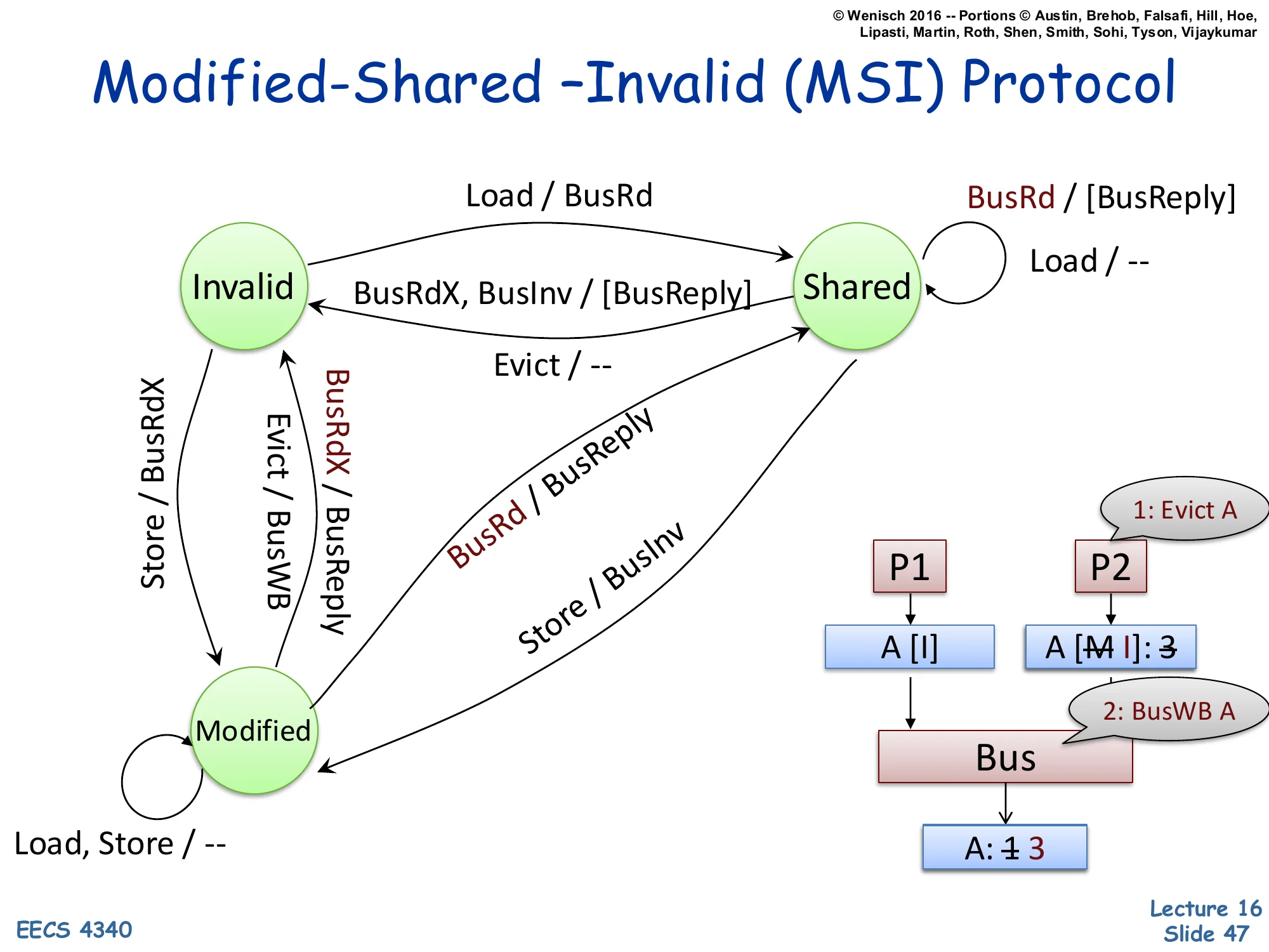
Show slide text
Modified-Shared –Invalid (MSI) Protocol
New transition: Modified → Invalid on Evict / BusWB (write back dirty data).
Example trace:
P1 P2 (Evict A) ▼ ▼ A [I] A [M→I]: 3 │ │ 2: BusWB A │ ▼ └──── Bus ◄────────┘ │ ▼ A: 1→3When a Modified line is evicted (capacity replacement or explicit cache flush), the protocol cannot drop it silently — it holds the only valid copy, and discarding it would lose the write. The evict triggers BusWB (bus writeback): the dirty line is written back to memory, then the cache transitions Modified → Invalid. Memory updates from stale 1 to current 3. After the writeback, memory is clean and authoritative; future readers can be satisfied from memory directly. This is the asymmetry with write-through caches, which keep memory always up to date but at the cost of every store causing bus traffic. Write-back amortizes by writing to memory only on eviction or coherence demand. The complete MSI state machine is now done — slide 48 summarizes.
MSI Protocol Summary
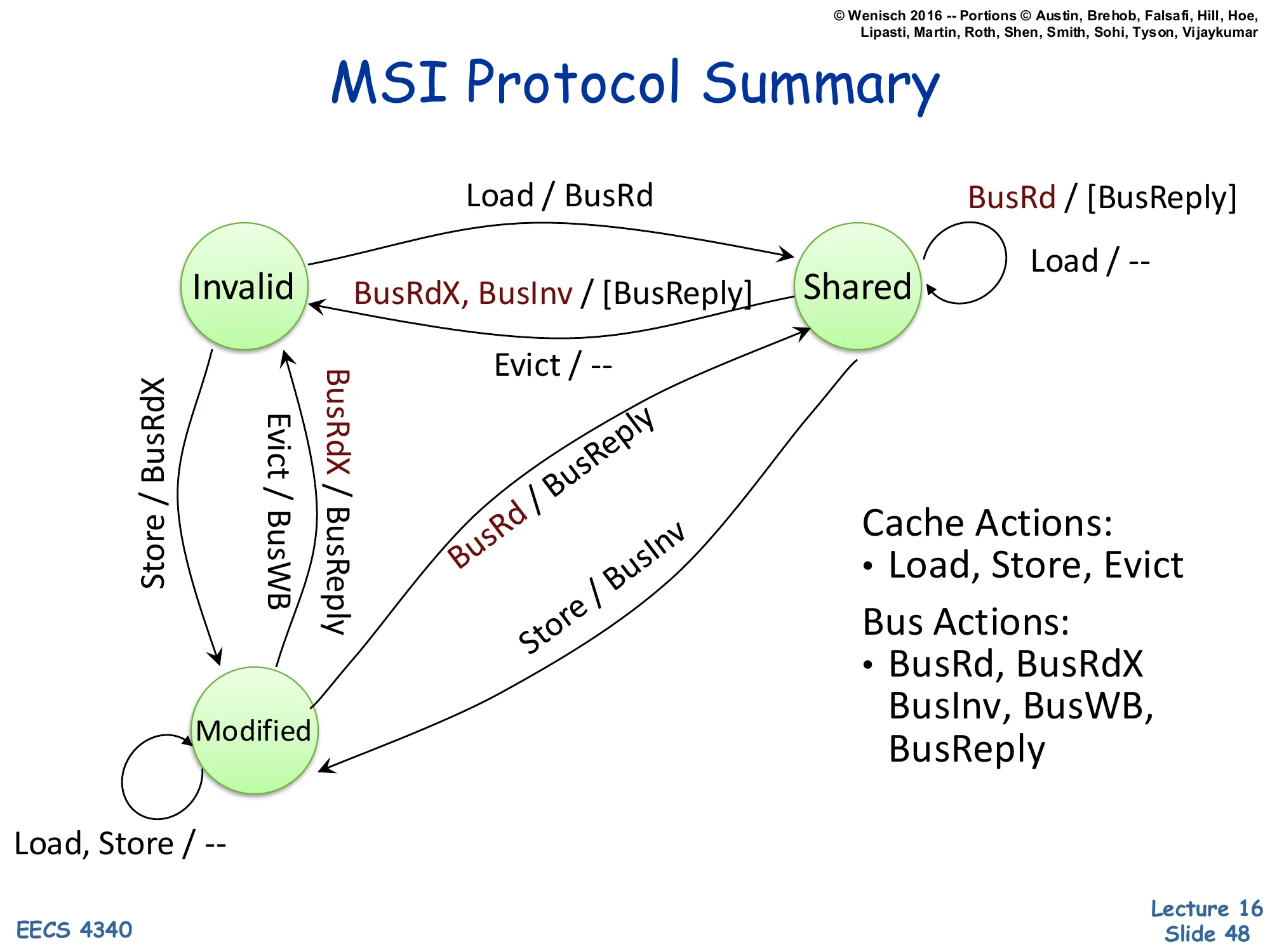
Show slide text
MSI Protocol Summary
State machine summary: states Invalid, Shared, Modified with transitions:
- I → S on Load / BusRd
- I → M on Store / BusRdX
- S → M on Store / BusInv
- S → I on Evict / — or snooped BusRdX or BusInv / [BusReply]
- M → S on snooped BusRd / BusReply
- M → I on Evict / BusWB or snooped BusRdX / BusReply
- Self-loops in S: Load / —, snooped BusRd / [BusReply]
- Self-loops in M: Load, Store / —
Cache Actions: Load, Store, Evict
Bus Actions: BusRd, BusRdX, BusInv, BusWB, BusReply
The complete MSI protocol in one diagram. Three states, three processor actions, five bus messages. The invariants worth memorizing: (1) at most one cache may hold a line in Modified; (2) any number of caches may hold a line in Shared; (3) Shared implies memory is clean; (4) Modified implies memory is stale. The write-runs-broadcast policy: every write either generates BusInv (S→M) or BusRdX (I→M, or M→I in another cache) on the bus. The read-runs-broadcast on miss policy: a load generates BusRd only on a miss. MESI adds an Exclusive state — the same as Modified but with memory still clean — to handle the read-then-write pattern: a single reader who later writes can avoid the BusInv because no other cache holds the line. MOESI adds Owned to allow cache-to-cache transfer of dirty data. All variants share the same MSI skeleton.
Memory Consistency Model
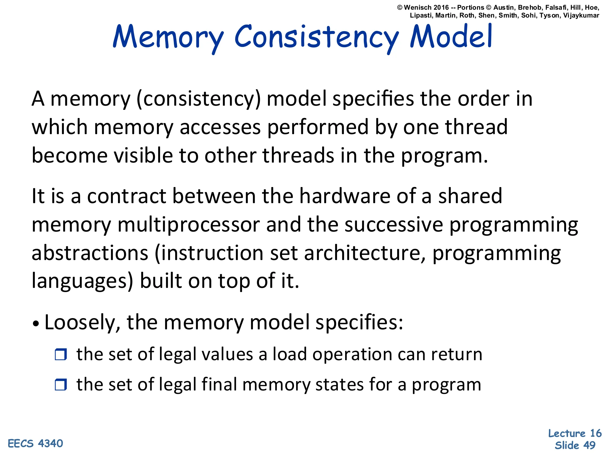
Show slide text
Memory Consistency Model
A memory (consistency) model specifies the order in which memory accesses performed by one thread become visible to other threads in the program.
It is a contract between the hardware of a shared memory multiprocessor and the successive programming abstractions (instruction set architecture, programming languages) built on top of it.
- Loosely, the memory model specifies:
- the set of legal values a load operation can return
- the set of legal final memory states for a program
Coherence says that all caches eventually agree on the value of any single address. Consistency is the harder property: it specifies how loads and stores to different addresses are ordered with respect to each other across threads. The classic example: thread A does x = 1; r1 = y; and thread B does y = 1; r2 = x;. Sequential consistency (Lamport, 1979) demands that some single global interleaving exists that explains every observed (r1, r2). Real hardware implements weaker models — Total Store Ordering (x86), Release Consistency (ARM), or RISC-V’s RVWMO — that allow more reordering for performance and require explicit fence instructions to recover ordering when needed. The slide emphasizes that the consistency model is a contract: hardware promises a specific set of legal observations, and software (compilers, language runtimes) must insert fences and atomics so that programs depend only on what the contract guarantees. Mismatched assumptions here are the source of many concurrency bugs.
Interconnection Networks
Interconnection Networks — Definition
Show slide text
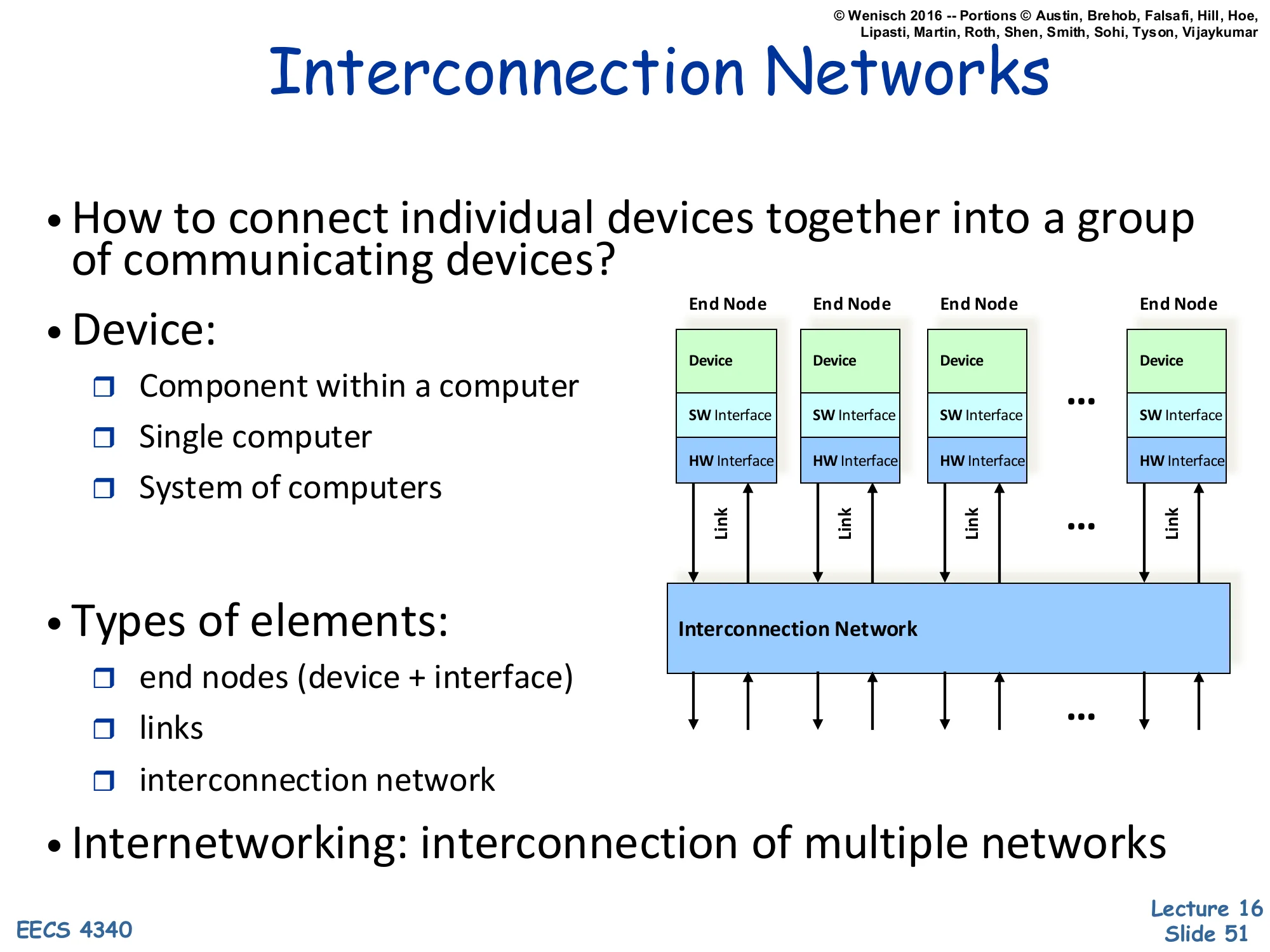
Interconnection Networks
- How to connect individual devices together into a group of communicating devices?
- Device:
- Component within a computer
- Single computer
- System of computers
Diagram: multiple End Nodes (each with Device, SW Interface, HW Interface) connected via Links to a shared Interconnection Network.
- Types of elements:
- end nodes (device + interface)
- links
- interconnection network
- Internetworking: interconnection of multiple networks
An interconnection network is the substrate that lets multiple devices communicate. The slide gives a deliberately scale-free definition: a ‘device’ can be a functional unit on a chip, an entire workstation, or a whole datacenter. The structural decomposition is consistent across scales — every interconnect has end nodes (the things being connected, with their software and hardware interfaces), links (the physical wires/fibers/buses), and a network (the topology and switching elements that route data between nodes). The term internetworking (interconnection of multiple networks) is what the modern internet does — TCP/IP routes between Ethernet LANs, cellular networks, satellite links, etc. This slide sets up the next several to drill into different scales: on-chip networks (millimeters), system-area networks (meters), local-area networks (kilometers), and wide-area networks (thousands of kilometers).
Interconnection Networks — Design Goals
Show slide text
Interconnection Networks
- Interconnection networks should be designed
- to transfer the maximum amount of information
- within the least amount of time (and cost, power constraints)
- so as not to bottleneck the system
The single-line design objective is unsurprising — maximize information per second under cost and power constraints. The pragmatic version is more nuanced: interconnects almost always become bottlenecks because compute scales faster than communication. On-chip, cores grew faster than bus bandwidth, forcing the move from buses to crossbars to meshes (slides 61–65). Off-chip, processors ran ahead of pin bandwidth, motivating optical interconnects, on-package HBM, and chiplet packaging. The ‘so as not to bottleneck the system’ phrasing is the practical one: the interconnect should not be the slowest link in the chain. The next several slides quantify this by classifying networks by scale (OCN, SAN, LAN, WAN) and walking through the tradeoffs that make each scale’s interconnect look the way it does.
Types of Interconnection Networks — OCNs
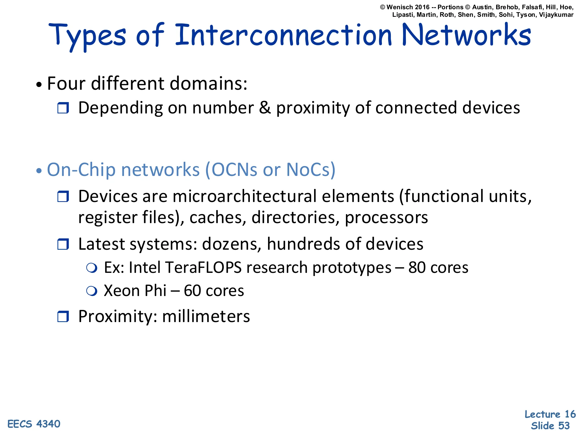
Show slide text
Types of Interconnection Networks
-
Four different domains:
- Depending on number & proximity of connected devices
-
On-Chip networks (OCNs or NoCs)
- Devices are microarchitectural elements (functional units, register files), caches, directories, processors
- Latest systems: dozens, hundreds of devices
- Ex: Intel TeraFLOPS research prototypes – 80 cores
- Xeon Phi – 60 cores
- Proximity: millimeters
On-chip networks (OCNs) or Network-on-Chip (NoCs) are the smallest scale of interconnect. Devices are tens to hundreds of microarchitectural blocks within a single chip — caches, directory slices, compute cores, register files. Distances are on the order of millimeters. Examples: Intel’s TeraFLOPS research chip (2007) had 80 simple cores tied by a 2D mesh; Xeon Phi (Knights Corner/Landing) had 60+ cores with a ring or mesh interconnect. The constraints on OCNs are very different from off-chip networks: wire bandwidth is plentiful but routing is constrained by metal layers; latencies are 1–10 cycles per hop; and area/power overhead must stay under 10–15% of the chip. The next slides cover SANs, LANs, and WANs at increasingly large scales.
System/Storage Area Networks (SANs)
Show slide text
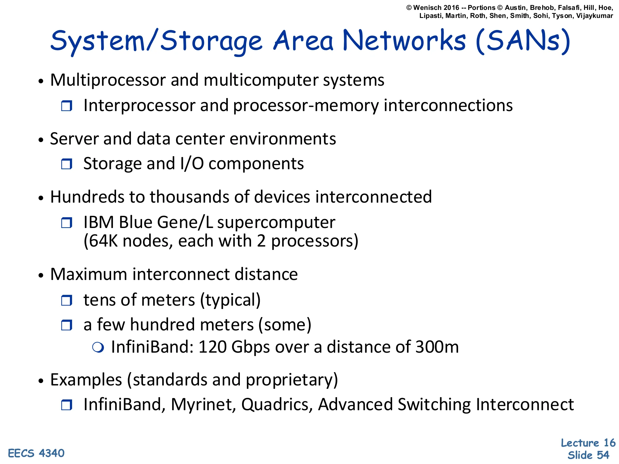
System/Storage Area Networks (SANs)
- Multiprocessor and multicomputer systems
- Interprocessor and processor-memory interconnections
- Server and data center environments
- Storage and I/O components
- Hundreds to thousands of devices interconnected
- IBM Blue Gene/L supercomputer (64K nodes, each with 2 processors)
- Maximum interconnect distance
- tens of meters (typical)
- a few hundred meters (some)
- InfiniBand: 120 Gbps over a distance of 300m
- Examples (standards and proprietary)
- InfiniBand, Myrinet, Quadrics, Advanced Switching Interconnect
System Area Networks (SANs) connect machines within a single rack, room, or building — typically in a server cluster, supercomputer, or storage system. Distance scale: tens to a few hundred meters. Device count: hundreds to thousands. Example: IBM Blue Gene/L scaled to 64K dual-processor nodes via custom torus and tree networks. InfiniBand is the main standardized SAN, providing 120 Gbps over up to 300m with sub-microsecond latency — used in HPC and high-end financial-services clusters. Myrinet, Quadrics, and Advanced Switching Interconnect were earlier or competing standards. SANs sit in a sweet spot between OCNs (limited to one die) and LANs (built for autonomous machines): they assume tightly-coupled, cooperating nodes with predictable workloads, allowing them to use lossless flow control, RDMA, and very low message latencies that wouldn’t scale to the open internet.
Local Area Networks (LANs)
Show slide text
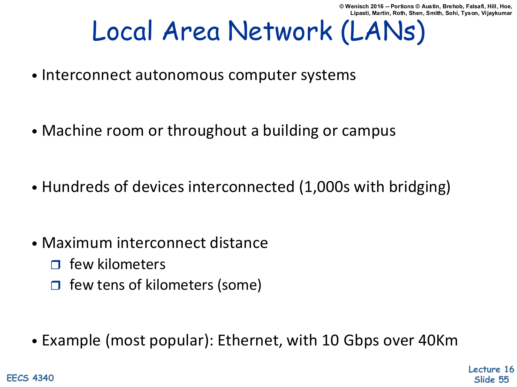
Local Area Network (LANs)
- Interconnect autonomous computer systems
- Machine room or throughout a building or campus
- Hundreds of devices interconnected (1,000s with bridging)
- Maximum interconnect distance
- few kilometers
- few tens of kilometers (some)
- Example (most popular): Ethernet, with 10 Gbps over 40Km
Local Area Networks (LANs) connect autonomous computers — independent machines that don’t share memory or coherence state — across a building or campus. Hundreds of devices natively, thousands with bridging/switching. Distances: a few kilometers, occasionally tens. Ethernet is the dominant standard, and its progression from 10 Mbps shared bus (1980s) to 10 Gbps over 40 km on optical fiber demonstrates how a single LAN technology can scale 1000× in bandwidth and 100× in distance over four decades by replacing the physical layer (twisted-pair → coax → fiber) and the access protocol (CSMA/CD → switched). LANs differ from SANs in that they don’t assume cooperating endpoints — they use best-effort delivery, must tolerate hostile neighbors, and use heavyweight protocols like TCP for reliability. They’re orders of magnitude higher latency than SANs (microseconds at best, often milliseconds) but vastly more scalable in node count and reach.
Wide Area Networks (WANs)
Show slide text
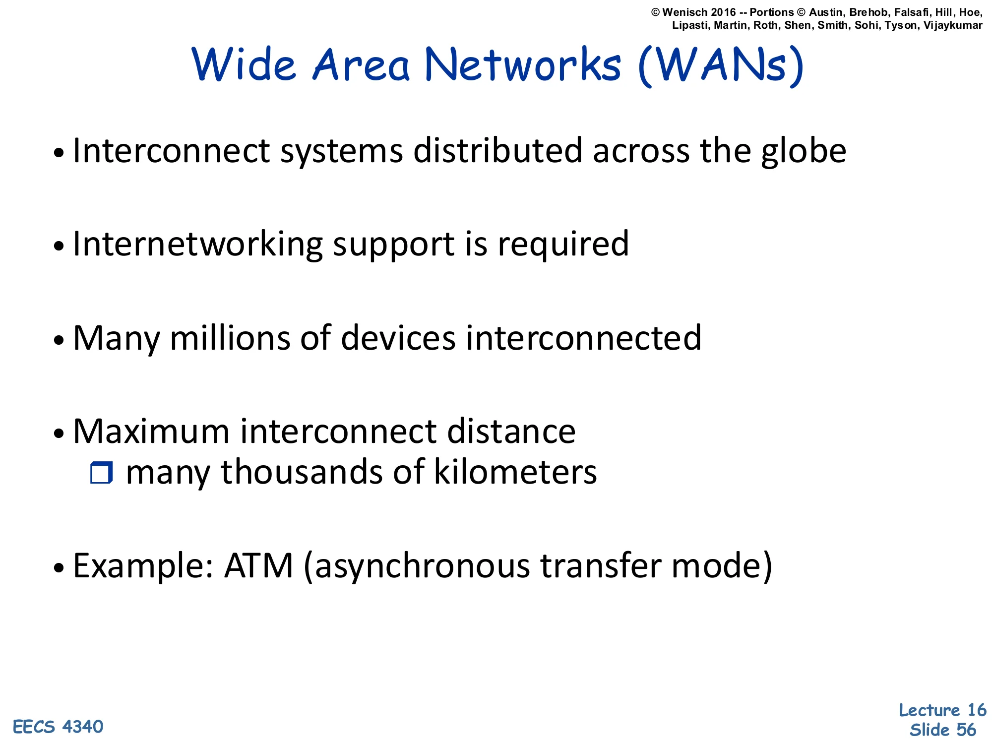
Wide Area Networks (WANs)
- Interconnect systems distributed across the globe
- Internetworking support is required
- Many millions of devices interconnected
- Maximum interconnect distance
- many thousands of kilometers
- Example: ATM (asynchronous transfer mode)
Wide Area Networks (WANs) connect systems across cities, continents, and oceans. The internet is the canonical WAN. Tens of millions to billions of devices; distances of thousands of kilometers; latencies bounded by speed of light (round-trip from coast-to-coast US is ~70 ms minimum). WANs require internetworking — forwarding packets across multiple interconnected networks of different types (Ethernet LANs, fiber backbones, cellular RANs, satellite links). This is what TCP/IP solves. ATM (Asynchronous Transfer Mode) is the example given on the slide — a fixed-length-cell switching technology that was widely deployed in telco backbones in the 1990s but largely displaced by IP-over-fiber by the 2010s. Modern WAN technology is dominated by IP, MPLS, BGP, and Ethernet at scale.
Interconnection Network Domains — Comparison
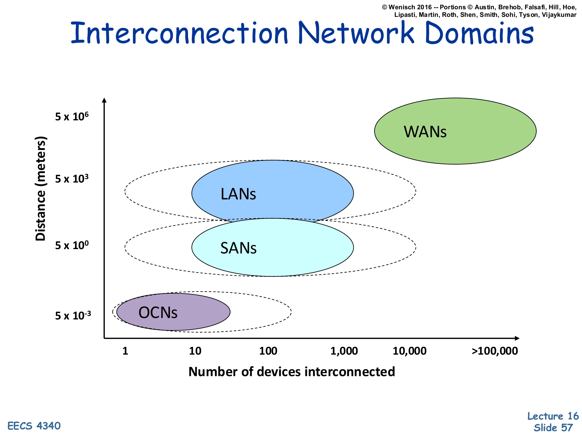
Show slide text
Interconnection Network Domains
Scatter plot: Distance (meters, log scale) vs. Number of devices interconnected (1 to >100,000):
- OCNs: ~5×10⁻³ m, 1–10 devices
- SANs: ~5×10⁰ m, ~10–1,000 devices
- LANs: ~5×10³ m, ~100–10,000 devices
- WANs: ~5×10⁶ m, >100,000 devices
The graphical summary places each interconnect class on a 2-D plot of distance vs. device count, both axes log-scaled. The four classes occupy roughly diagonal bands: as you go further (taller on the y-axis), you tend to connect more devices (further right on the x-axis). The progression spans nine orders of magnitude in distance (millimeters to thousands of kilometers) and five in device count (1 to >100,000). The dotted contours show that domains overlap — a small SAN and a small LAN can have similar device counts, distinguished mainly by latency requirements and cooperative vs. autonomous endpoints. The plot is useful for picking the right technology: don’t run a directory protocol over a WAN, and don’t run TCP between cores on the same chip.
On-Chip Networks (OCN or NoCs)
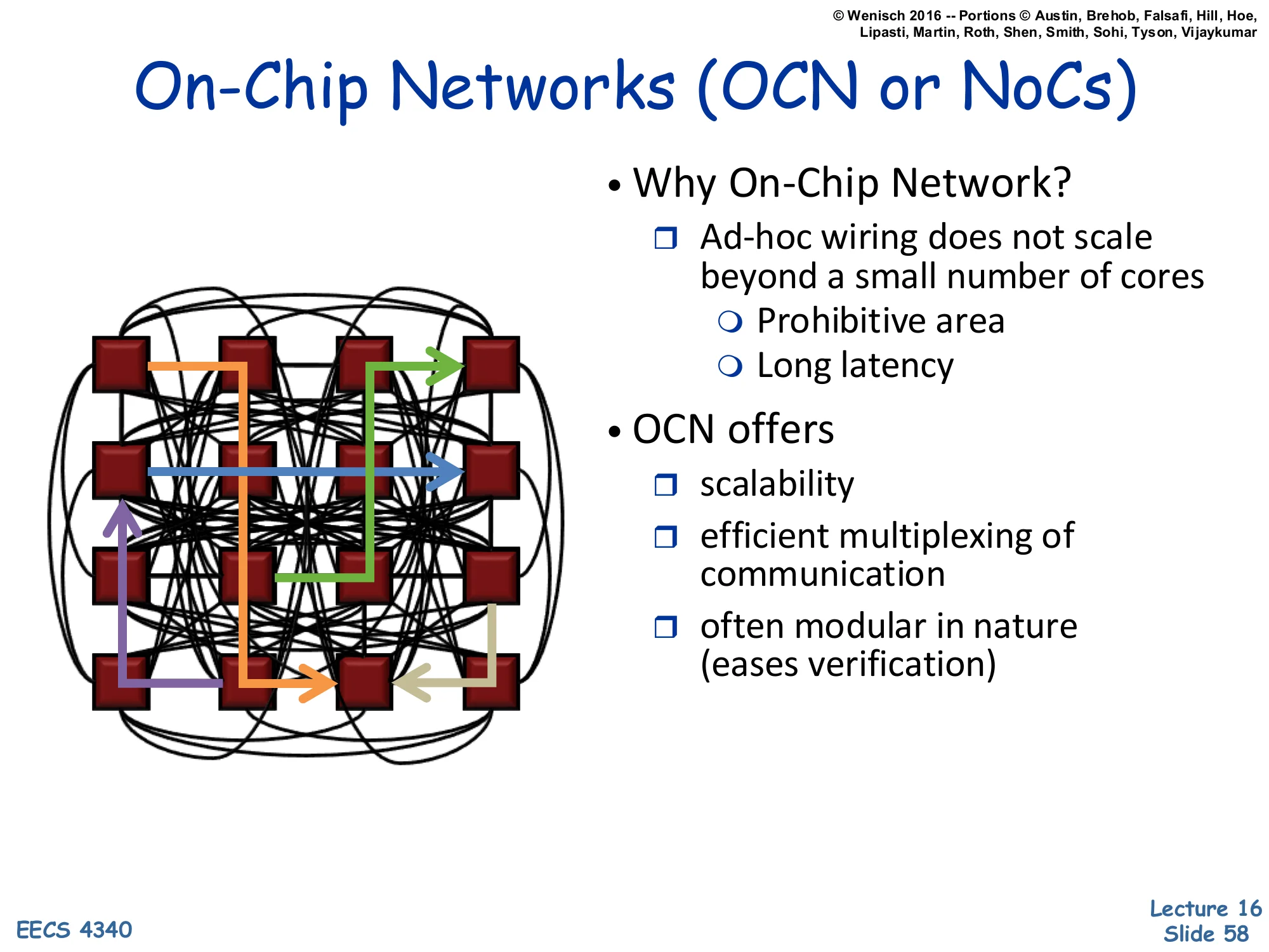
Show slide text
On-Chip Networks (OCN or NoCs)
Diagram: a 4×4 grid of cores tied together by a complex routing network with directional flows.
- Why On-Chip Network?
- Ad-hoc wiring does not scale beyond a small number of cores
- Prohibitive area
- Long latency
- Ad-hoc wiring does not scale beyond a small number of cores
- OCN offers
- scalability
- efficient multiplexing of communication
- often modular in nature (eases verification)
Once core count exceeds about 4–8, ad-hoc point-to-point wiring becomes untenable: a fully-connected n-core mesh would require n(n−1)/2 wires (quadratic), each long, slow, and routed across the die’s metal layers. The chip area, latency, and complexity all explode. Networks-on-Chip (NoCs) replace ad-hoc wiring with a regular topology — usually a 2D mesh, ring, or hierarchical tree — where each node has a router with a few fixed ports. Scalability comes from logarithmic-or-linear hop counts and the ability to time-share each link among many flows. Modularity comes from each tile (core + L1 + router) being identical, simplifying physical design, testing, and verification. The price is per-hop latency: a 4-cycle router × 8 hops = 32 cycles for a coast-to-coast on-chip message — slower than a direct wire but vastly more scalable.
Differences between on-chip and off-chip networks
Show slide text
Differences between on-chip and off-chip networks
- Significant research in multi-chassis interconnection networks (off-chip)
- Supercomputers
- Clusters of workstations
- Internet routers
- Leverage research and insight but…
- Constraints are different
Off-chip networks have been studied since the 1970s — supercomputer interconnects (Cray, IBM Blue Gene), workstation clusters (Berkeley NOW), and internet routers all share theoretical foundations like topology theory, flow control, and routing algorithms. NoC designers can leverage that research, but the physical and economic constraints differ significantly. On-chip wires are short, plentiful, and noise-resilient, but routing is constrained by chip metal layers and ‘do not route over dense logic’ rules. Power is the dominant constraint on-chip, while bandwidth (pin count) is the dominant constraint at chip boundaries. Storage in routers (input buffers, virtual channels) is precious on-chip. Latency budgets are tens of cycles instead of microseconds. The next slide makes these differences concrete.
Off-chip vs. on-chip
Show slide text
Off-chip vs. on-chip
- Off-chip: I/O bottlenecks
- Pin-limited bandwidth
- Inherent overheads of off-chip I/O transmission
- On-chip
- Wiring constraints
- Metal layer limitations
- Horizontal and vertical layout
- Short, fixed length
- Repeater insertion limits routing of wires
- Avoid routing over dense logic
- Impact wiring density
- Power
- Consume 10-15% or more of die power budget
- Latency
- Different order of magnitude
- Routers consume significant fraction of latency
- Wiring constraints
Off-chip is pin-limited: a chip has only so many balls (typically 1000–5000), and high-speed serial links per pin top out at tens of Gbps. Total off-chip bandwidth is therefore severely bounded, even as on-chip compute grows. Off-chip transmission also has fixed overheads (SerDes, encoding, error detection) that don’t scale down with message size. On-chip is wire-constrained: only a few layers of metal are available, wires must be routed around dense logic, and signal repeaters limit how long a wire can run before regeneration. Power for the on-chip network is typically 10–15% of the die’s total budget — non-trivial. Latency for on-chip routers is a few cycles per hop, vs. tens to hundreds of nanoseconds for an off-chip link. These constraints shape NoC design choices: shallow router pipelines, simple flow control (credit-based), small buffers, and careful floor-planning.
On-Chip Network Evolution
Show slide text
On-Chip Network Evolution
- Ad hoc wiring
- Small number of nodes
- Buses and Crossbars
- Simplest variant of on-chip networks
- Low core counts
- Like traditional multiprocessors
- Bus traffic quickly saturates with a modest number of cores
- Crossbars: higher bandwidth
- Poor area and power scaling
On-chip interconnect evolution mirrors the historical SMP-to-NUMA arc but on a much shorter timescale. Ad-hoc wiring worked when chips had two or four functional units. Buses are the simplest scalable solution: one shared signal carries all traffic, with arbitration deciding who transmits. Buses reuse the snooping coherence intuition (slide 35) and work well up to ~8 cores, beyond which contention saturates the bandwidth. Crossbars — fully-connected switches between n ports — provide n-way concurrent communication but their area scales as n2 (each input has a path to each output) and their power scales similarly because every crosspoint is a multiplexer. Sun’s Niagara 2 (slide 62) used an 8×9 crossbar, which was already roughly the size of a core. Beyond ~16 cores, both buses and crossbars become prohibitive, motivating mesh and ring topologies (slides 63–65).
Multicore Examples (1) — Sun Niagara
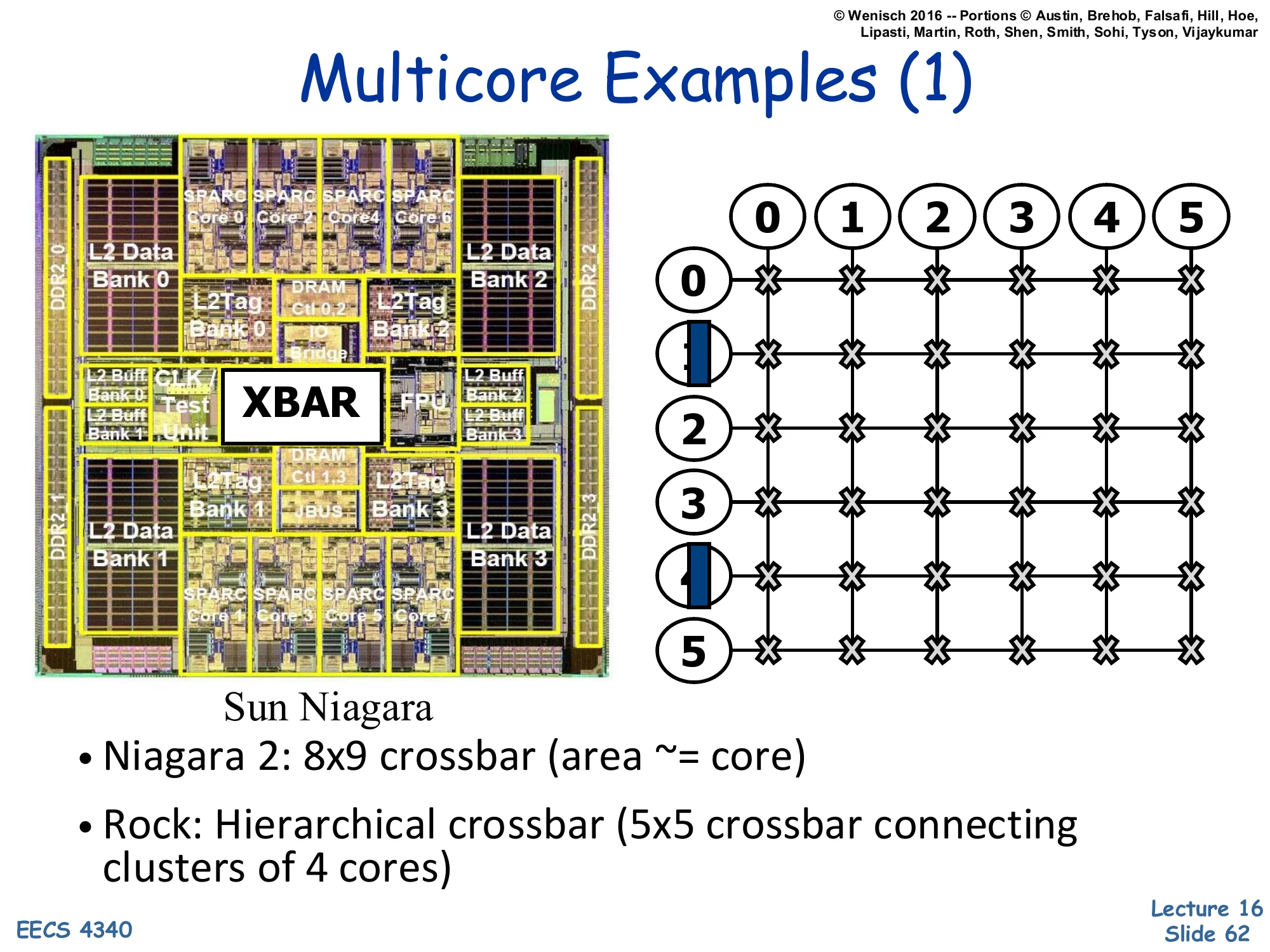
Show slide text
Multicore Examples (1)
Left: die photo of Sun Niagara with SPARC cores arranged around an XBAR (crossbar) and L2 Data/Tag banks. Right: 6×6 grid of crossbars showing hierarchical interconnection.
Sun Niagara
- Niagara 2: 8×9 crossbar (area ≈ core)
- Rock: Hierarchical crossbar (5×5 crossbar connecting clusters of 4 cores)
Sun’s Niagara 1 (UltraSPARC T1) and Niagara 2 (T2) are textbook examples of crossbar-based on-chip interconnects. Niagara 2 had 8 cores with 4-way SMT each, totaling 64 hardware threads, all connected to 8 shared L2 cache banks via an 8×9 crossbar (the 9th port being for I/O). The slide highlights that this crossbar’s area is roughly the same as one core — a striking illustration of how crossbar area dominates as port counts grow. Sun’s Rock processor (cancelled) tried hierarchical crossbars: a 5×5 crossbar at the top level connected clusters of 4 cores, where each cluster had its own internal crossbar. This breaks the n2 scaling into a tree of smaller crossbars, but adds latency for cross-cluster traffic. Hierarchical interconnect is a recurring theme in larger many-cores.
Multicore Examples (2) — IBM Cell
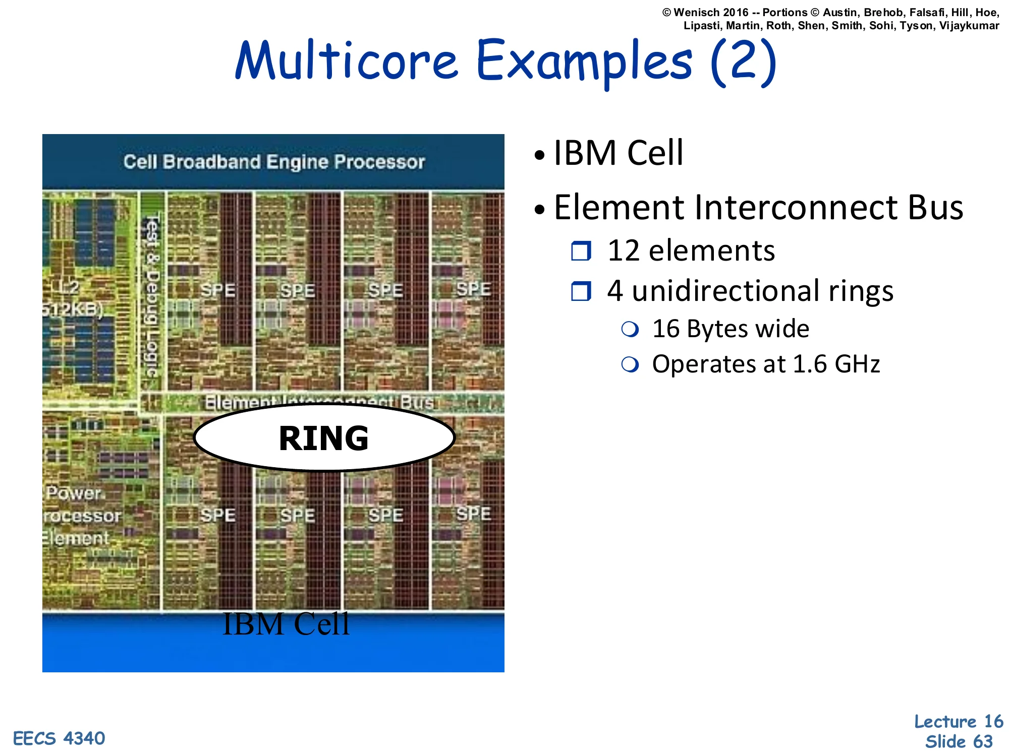
Show slide text
Multicore Examples (2)
Image: die photo of the IBM Cell Broadband Engine Processor showing PowerPC core, 8 SPEs, and a central RING.
- IBM Cell
- Element Interconnect Bus
- 12 elements
- 4 unidirectional rings
- 16 Bytes wide
- Operates at 1.6 GHz
The IBM Cell processor (used in the PlayStation 3 and HPC clusters) takes a different topological approach: a ring. The Element Interconnect Bus (EIB) is actually four parallel unidirectional rings — two clockwise, two counterclockwise — each 16 bytes wide and clocked at 1.6 GHz, giving aggregate bandwidth of 4 × 16 × 1.6 = ~100 GB/s. The 12 ‘elements’ are the PowerPC PPE (general-purpose core), 8 SPEs (Synergistic Processor Elements — vector accelerators), the memory interface, and I/O controllers. Rings have a lovely property: they scale linearly in area (each node has only 2 in/out ports regardless of total count), and routing is trivial (always go in the direction with fewer hops). The downside is that average hop count grows as n/4, so latency scales with size. Rings dominated mid-2000s many-core designs (Cell, Intel Xeon Phi, Larrabee) before mesh topologies took over for higher core counts.
Many Core Example — Intel TeraFLOPS
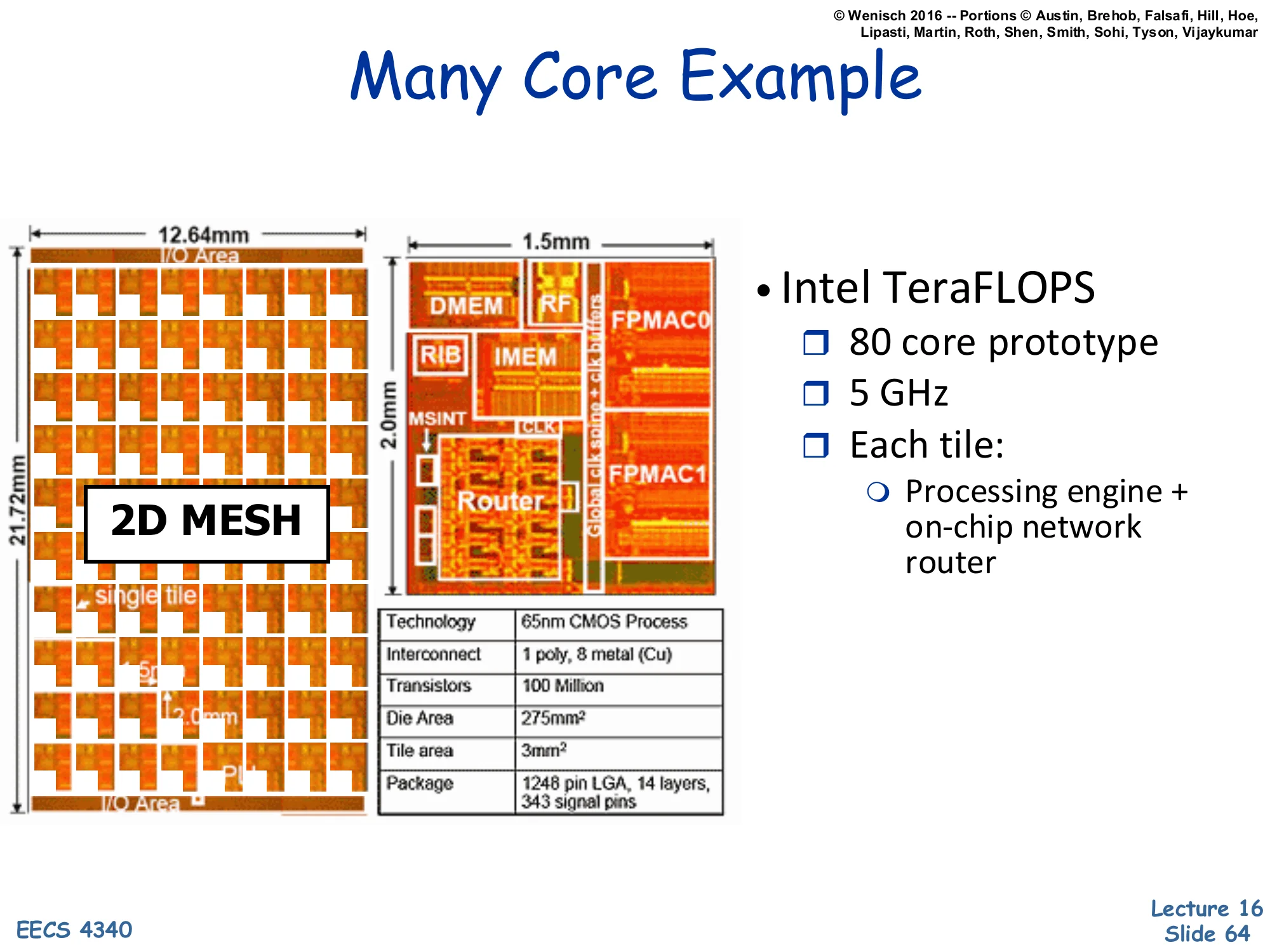
Show slide text
Many Core Example
Left: 12.64 mm × 21.72 mm die organized as a 2D MESH of 80 tiles. Right: zoomed tile (1.5 × 2.0 mm) showing DMEM, IMEM, RIB, MSINT, FPMAC0, FPMAC1, and Router.
- Intel TeraFLOPS
- 80 core prototype
- 5 GHz
- Each tile:
- Processing engine + on-chip network router
Specs table: 65 nm CMOS Process, 1 poly, 8 metal (Cu) interconnect, 100 Million Transistors, 275 mm² Die Area, 3 mm² Tile area, 1248 pin LGA, 14 layers, 343 signal pins.
Intel’s TeraFLOPS Research Chip (Polaris, 2007) is the iconic example of mesh-based many-core architecture. It packs 80 cores into a 2D mesh on a 275 mm² die at 65 nm, hitting >1 TFLOPS at 5 GHz — a milestone for 2007. Each tile is a 3 mm² unit containing two FPMAC (floating-point multiply-accumulate) units, instruction memory, data memory, a routing-instruction buffer (RIB), a mesh interface (MSINT), and a router. The 2D mesh topology means each tile has ports to 4 neighbors (north/south/east/west) plus a local injection port — 5 ports per router. Hop count scales as n for an n-tile mesh, much better than a ring’s n/2. The chip never shipped as a product, but its architecture directly informed Xeon Phi’s mesh interconnect (slide 65 hints at this with Intel SCC). Modern multi-core CPUs (50+ cores) almost universally use 2D mesh on-chip networks.
Many-Core Example (2) — Intel SCC
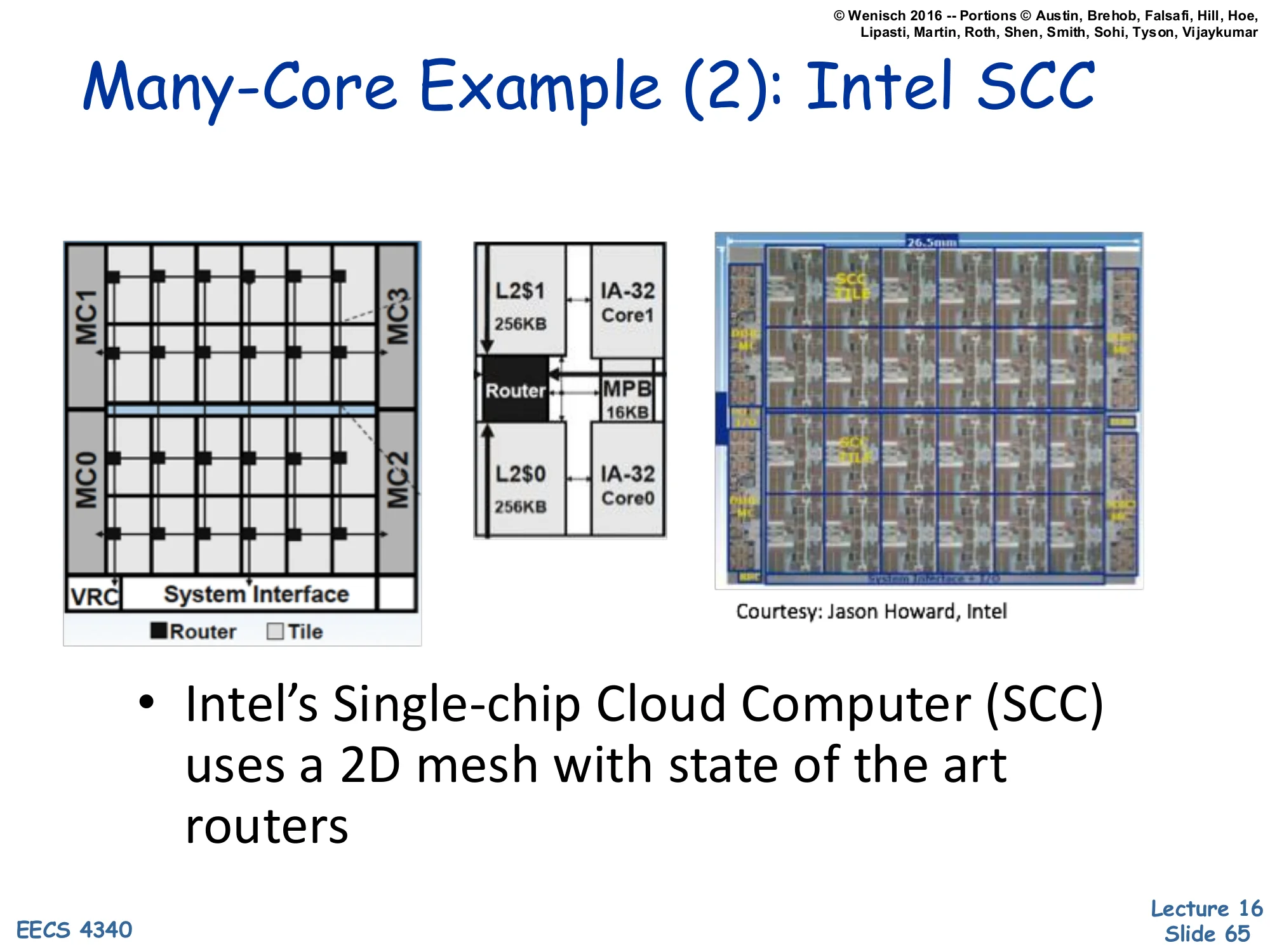
Show slide text
Many-Core Example (2): Intel SCC
Left: 4×6 tile mesh layout with 4 memory controllers (MC0–MC3) at the corners and a System Interface at the bottom. Each tile has a Router and Tile. Middle: a tile zoom showing two IA-32 cores (Core0/Core1), each with its own L2 cache (256KB), a shared MPB (Message Passing Buffer, 16KB), and a Router. Right: chip photo (26.5 mm wide). Courtesy: Jason Howard, Intel.
- Intel’s Single-chip Cloud Computer (SCC) uses a 2D mesh with state of the art routers
Intel’s Single-chip Cloud Computer (SCC, 2010) is a research chip that pushes the multicore-NoC idea further. 24 tiles (each with 2 IA-32 P54C cores) tile a 4×6 mesh, totaling 48 x86 cores. Four memory controllers (MC0–MC3) are placed at the corners to spread DRAM bandwidth. Each tile has its own L2 cache and a 16 KB Message Passing Buffer (MPB) — the SCC notably runs without hardware cache coherence between tiles, instead exposing the MPB as a software-managed shared scratchpad. This deliberately treats the on-chip network like a cluster: a shared-memory programmer must do their own coherence via explicit MPB messages, much like programming a distributed system in miniature. The SCC was a research vehicle for studying software coherence and per-core power gating at scale. The architecture influenced later Xeon Phi designs and is a useful reminder that the hardware-coherence-everywhere approach is not the only way to build a many-core.
Performance and Cost
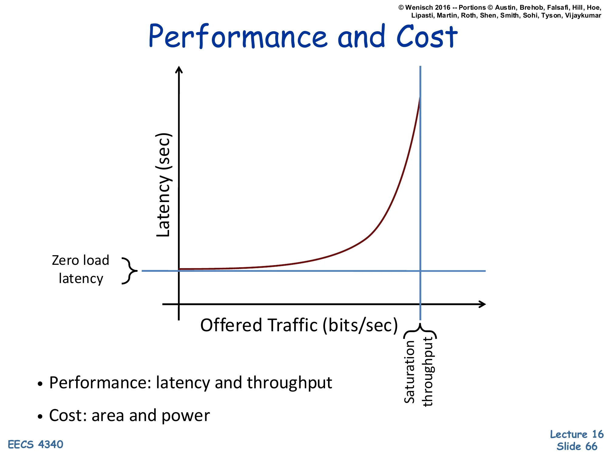
Show slide text
Performance and Cost
Plot: Latency (sec) on y-axis vs. Offered Traffic (bits/sec) on x-axis. The latency curve starts flat at the Zero load latency value, then rises sharply as offered traffic approaches the Saturation throughput vertical asymptote.
- Performance: latency and throughput
- Cost: area and power
The performance of any interconnection network is captured by this canonical throughput-latency curve, identical in shape to queueing theory’s M/M/1 response curve. At low offered traffic, latency equals the zero-load latency — the minimum time for one packet to traverse the empty network (router pipeline + wire delay × hops). As offered traffic increases, queueing at routers begins to add waiting time, and latency rises gracefully. As traffic approaches the saturation throughput — the maximum rate the network can sustain, bounded by the bisection bandwidth or hottest-link bandwidth — latency diverges to infinity, because incoming traffic exceeds drain rate and queues grow unbounded. The two performance metrics are zero-load latency (best case) and saturation throughput (capacity). The two cost metrics are area (silicon real estate consumed by routers and wires) and power (dynamic + static dissipation). Network designers trade these four against each other across topology, routing algorithm, flow control, and buffer sizing.
Applications & Architectures
Data Center Applications
Show slide text
Data Center Applications
- Historically, primary market for multiprocessor systems
- Examples:
- Database systems: Oracle, DB2, SQLServer, PostGres, MySQL
- Business apps: SAP, BAAN, PeopleSoft
- Data analysis: large scale graph processing
- Web-servers
- Static content
- Dynamic content: database integration + business logic
- Web 2.0: user-supplied content
- Infrastructure apps: J2EE
Before consumer multicore, the multiprocessor market was almost entirely server-side. The five categories on the slide span the workloads that justified building large SMPs and NUMA machines through the 1990s and 2000s. Databases (OLTP and OLAP) are the canonical multiprocessor workload — they’re parallel within a query (multiple cores work on different rows or partitions) and across queries (many users hitting the same DB simultaneously). Business apps like SAP and PeopleSoft layer on top of databases, adding application-server tiers. Data analysis (especially graph processing on social networks) became dominant in the 2010s with Hadoop and Spark. Web servers — Apache, Nginx, Tomcat — handle thousands of concurrent connections on multicore machines. Infrastructure like J2EE provides middleware that wraps all of these. The common pattern: many independent client requests fanning out across many cores, with shared state in a database — the multiprocessor sweet spot.
Why Study Data Center Applications?
Show slide text
Why Study Data Center Applications?
- They are economically important
- They share characteristics of many other apps (filesystems, web search, etc.)
- The vendors have spent a lot of time optimizing (generally, they won’t have silly bottlenecks)
Three pragmatic reasons to study data-center workloads in an architecture course. Economic — datacenters are the multi-billion-dollar market for multiprocessor hardware; what runs there pays the R&D bills. Generalizable characteristics — the access patterns and bottlenecks (cold I-cache footprints, large TLB reach, deep call stacks, irregular memory) recur in filesystems, search engines, and middleware, so insights transfer broadly. Already optimized — vendors with multi-billion-dollar revenue (Oracle, Microsoft) have wrung the obvious bottlenecks out, so studying these workloads reveals the fundamental hardware-level limits rather than transient software problems. The slide’s implication: if you’re going to design hardware for the next decade, design for what these workloads actually do, not for synthetic benchmarks like SPEC. Architectural research has steadily shifted in this direction since the late 2000s.
Key Characteristics of Data Center Apps
Show slide text
Key characteristics
- Large, complex, monolithic software systems
- Designed for MP systems
- Clusters (distributed databases)
- Shared Memory
- Subsumes many OS functions
- File system
- Scheduling and multi-threading
- Memory management
- Designed for high reliability (ACID properties)
- Atomicity: a transaction happens or doesn’t
- Consistency: the state of the DB remains consistent
- Isolation: transactions are independent
- Durability: once performed, transactions are permanent
- Aside: we will see these ideas pop up in architecture context again with transactional memory
Data-center applications, especially databases, have several hardware-relevant characteristics. They’re huge (millions of lines, deep call stacks) — the I-cache sees a much larger working set than typical SPEC benchmarks. They’re designed for multiprocessing either via clusters (sharded databases like Cassandra, distributed query engines) or via shared memory (single-instance Oracle, Postgres). They replace OS functions with their own implementations — Oracle has its own buffer pool, scheduler, and lock manager — making the OS less of a bottleneck and the database more responsible for performance. The ACID properties (Atomicity, Consistency, Isolation, Durability) are the database correctness contract: they preview transactional memory, which is essentially ACID semantics applied to in-memory critical sections via hardware speculation. The aside at the bottom highlights that the same conceptual primitives recur at multiple layers of the system stack.
How Are Data Center Apps Different?
Show slide text
How are they different?
- Requires tuning: knowledge-intensive, difficult
- Competitive market: deliberate obfuscation/ benchmark gaming
- Large instruction footprints (I$ matters)
- Huge data footprints (TLBs matter)
- Weird access types (cross-endian, non-cacheable, etc.)
- Latency, not bandwidth bound
- Dynamic memory allocation, sometimes garbage collection
- More pointer-chasing, fewer arrays
- No single obvious “working set”
- multiple working sets with varying temporal locality
- Unpredictable sharing patterns
- Data & lock contention
This is a checklist of what makes server workloads architecturally different from SPEC and microbenchmarks. Large I-cache footprints mean the L1-I miss rate dominates rather than the D-cache; some servers see >10% of stalls from I-cache. Huge data footprints stress the TLB — page-table walks become a measurable cost, motivating large-page support and TLB prefetching. Latency-bound (not bandwidth-bound) means accelerating individual cache miss handling helps, but adding more memory channels doesn’t. Pointer-chasing (linked lists, B-tree internal nodes) defeats hardware stride prefetchers designed for arrays. No single working set means hierarchical caches with different policies per level help. Unpredictable sharing and lock contention stress the coherence protocol with frequent invalidations. The architectural takeaways: servers need bigger TLBs, smarter prefetchers (correlation-based, not stride), aggressive memory-level parallelism, and efficient lock primitives — all very different design priorities than for desktop or HPC workloads.
Unconventional Parallel Architectures
Dataflow Architectures
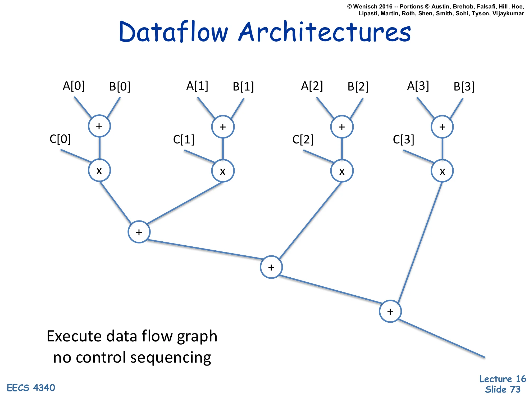
Show slide text
Dataflow Architectures
Diagram: a binary tree of operators computing ((A[0]+B[0])×C[0])+((A[1]+B[1])×C[1])+((A[2]+B[2])×C[2])+((A[3]+B[3])×C[3]). Leaves are operands, interior nodes are × and +.
Execute data flow graph no control sequencing
Dataflow architectures fire on data availability rather than program-counter advancement. Each operator (e.g., +, ×) is a node in a graph; it fires when all its input operands are ready, producing an output token that flows along edges to consume it. There is no global program counter and no instruction sequencing — parallelism is implicit and maximal. The example computes ∑i=03(Ai+Bi)×Ci as a tree: four +‘s and four בs can fire in parallel at the leaves; their outputs feed three more +‘s in two further parallel rounds. Dataflow machines (MIT Tagged-Token Dataflow, Manchester Dataflow Machine) were studied extensively in the 1980s but failed commercially because of token-matching overhead and the difficulty of handling memory state. The idea, however, lives on: Tomasulo’s algorithm is dataflow scheduling at the instruction level inside a conventional CPU, and modern ML compilers (XLA, MLIR) build dataflow graphs to optimize before lowering to hardware.
Systolic Arrays
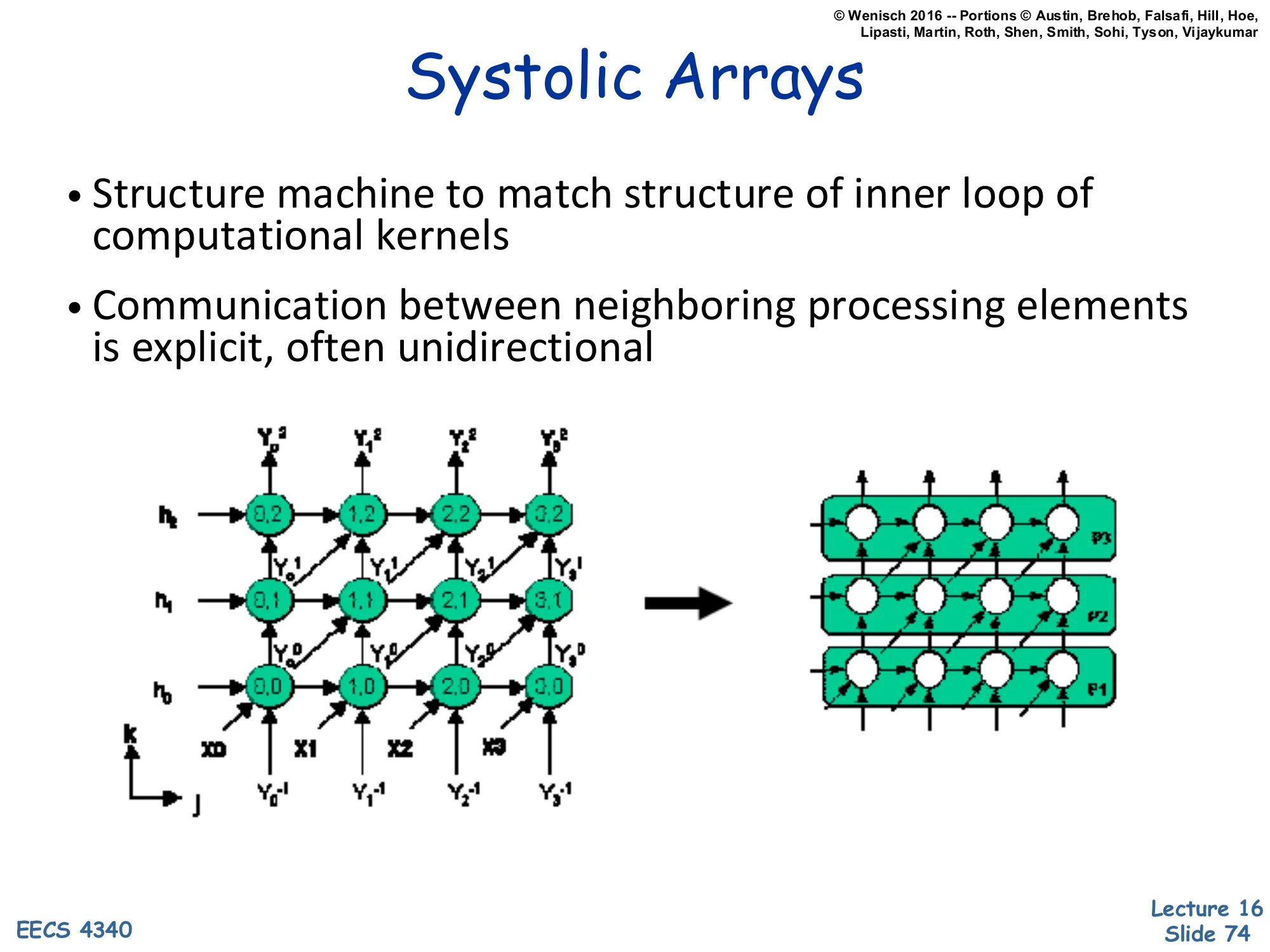
Show slide text
Systolic Arrays
- Structure machine to match structure of inner loop of computational kernels
- Communication between neighboring processing elements is explicit, often unidirectional
Left diagram: 4×3 grid of processing elements with input vectors X0–X3 entering from the bottom and h₀–h₂ entering from the left. Outputs Y₀⁻¹–Y₃⁻¹ at the bottom and Y₀²–Y₃² at the top, with diagonal flows. Right diagram: stylized rows P₁/P₂/P₃ of cells each connected to neighbors with directional arrows.
Systolic arrays match hardware structure to the loop nest of a computational kernel. Each processing element (PE) is simple — usually one multiply-accumulate operation per cycle — and PEs communicate only with immediate neighbors via explicit, often unidirectional links. Data flows through the array like a pulse (hence ‘systolic’, from cardiology), with results emerging on the far side. The classic example is matrix multiplication: a matrix A flows in from the left, B flows in from the bottom, partial sums of C accumulate at each PE, and after n cycles the answer pulses out the right. The key advantage: locality of communication keeps each PE simple, wires short, and clock frequency high. After a 1980s research wave (H.T. Kung’s seminal work), systolic arrays disappeared into specialty signal-processing chips — until Google’s TPU brought them back as the canonical ML matrix-multiply substrate. NVIDIA’s tensor cores and AMD’s matrix cores are similarly structured.
Concepts of Multiprocessors — Recap

Show slide text
Concepts of Multiprocessors
Parallel Programming Models
- Message passing, shared memory (pthreads and GPU)
Synchronization
- Locks, Lock-free structures, Transactional Memory
Coherency and Consistency
- Snooping and Directory-based Coherency
- Memory Consistency Models
Interconnection Networks
- On-chip and off-chip networks
Applications & Architectures
- Data center applications, MLPerf
Unconventional Parallel Architectures
- Dataflow architectures and systolic arrays
The closing slide reproduces slide 12 verbatim, framing the lecture as a tour of six themes. Looking back: Programming models (slides 13–24) — shared memory and message passing as the two fundamental abstractions, with GPUs as a SIMT-flavored variant. Synchronization (slides 25–30) — locks, barriers, the spin/block tradeoff, and the contention/multiprogramming challenges. Coherence and consistency (slides 31–49) — the MSI state machine in detail, snooping vs. directories, and the consistency-vs-coherence distinction. Interconnects (slides 50–66) — OCN, SAN, LAN, WAN scales and the latency/throughput design space. Applications (slides 67–71) — datacenter workloads as the architectural target. Unconventional architectures (slides 72–74) — dataflow and systolic, both alive today inside accelerators. The unifying lesson: parallelism is now the dominant lever for performance, and every layer of the system stack — programming languages, synchronization primitives, coherence protocols, interconnect topologies — has had to adapt.